ARM720T_LH79520 – Sharp LH79520 SoC with ARM720T
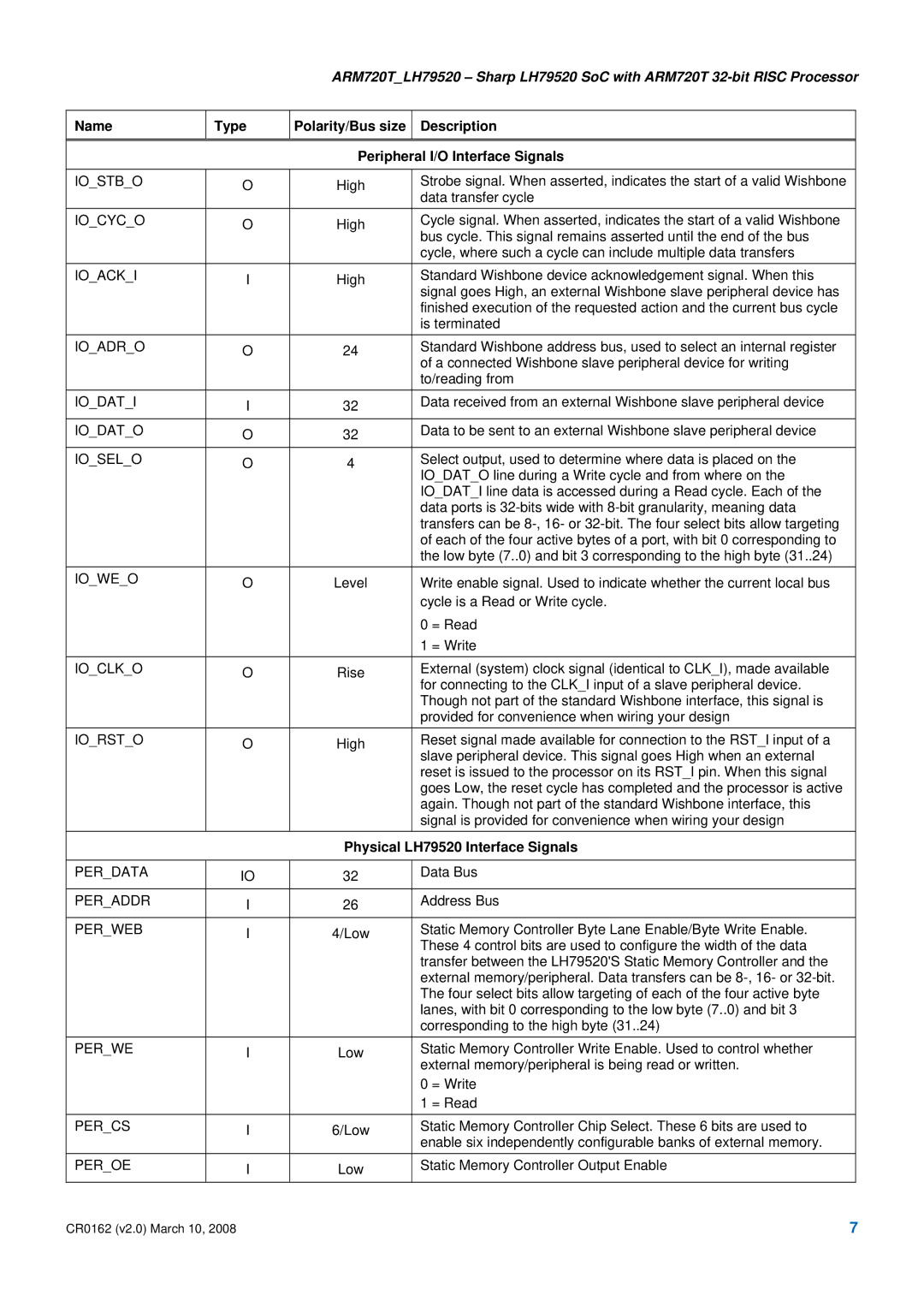
Name | Type | Polarity/Bus size | Description |
|
|
|
|
|
| Peripheral I/O Interface Signals | |
|
|
|
|
IO_STB_O | O | High | Strobe signal. When asserted, indicates the start of a valid Wishbone |
|
|
| data transfer cycle |
IO_CYC_O | O | High | Cycle signal. When asserted, indicates the start of a valid Wishbone |
|
|
| bus cycle. This signal remains asserted until the end of the bus |
|
|
| cycle, where such a cycle can include multiple data transfers |
IO_ACK_I | I | High | Standard Wishbone device acknowledgement signal. When this |
|
|
| signal goes High, an external Wishbone slave peripheral device has |
|
|
| finished execution of the requested action and the current bus cycle |
|
|
| is terminated |
IO_ADR_O | O | 24 | Standard Wishbone address bus, used to select an internal register |
|
|
| of a connected Wishbone slave peripheral device for writing |
|
|
| to/reading from |
IO_DAT_I | I | 32 | Data received from an external Wishbone slave peripheral device |
|
|
|
|
IO_DAT_O | O | 32 | Data to be sent to an external Wishbone slave peripheral device |
|
|
|
|
IO_SEL_O | O | 4 | Select output, used to determine where data is placed on the |
|
|
| IO_DAT_O line during a Write cycle and from where on the |
|
|
| IO_DAT_I line data is accessed during a Read cycle. Each of the |
|
|
| data ports is |
|
|
| transfers can be |
|
|
| of each of the four active bytes of a port, with bit 0 corresponding to |
|
|
| the low byte (7..0) and bit 3 corresponding to the high byte (31..24) |
IO_WE_O | O | Level | Write enable signal. Used to indicate whether the current local bus |
|
|
| cycle is a Read or Write cycle. |
|
|
| 0 = Read |
|
|
| 1 = Write |
IO_CLK_O | O | Rise | External (system) clock signal (identical to CLK_I), made available |
|
|
| for connecting to the CLK_I input of a slave peripheral device. |
|
|
| Though not part of the standard Wishbone interface, this signal is |
|
|
| provided for convenience when wiring your design |
IO_RST_O | O | High | Reset signal made available for connection to the RST_I input of a |
|
|
| slave peripheral device. This signal goes High when an external |
|
|
| reset is issued to the processor on its RST_I pin. When this signal |
|
|
| goes Low, the reset cycle has completed and the processor is active |
|
|
| again. Though not part of the standard Wishbone interface, this |
|
|
| signal is provided for convenience when wiring your design |
|
| Physical LH79520 Interface Signals | |
|
|
|
|
PER_DATA | IO | 32 | Data Bus |
|
|
|
|
PER_ADDR | I | 26 | Address Bus |
|
|
|
|
PER_WEB | I | 4/Low | Static Memory Controller Byte Lane Enable/Byte Write Enable. |
|
|
| These 4 control bits are used to configure the width of the data |
|
|
| transfer between the LH79520'S Static Memory Controller and the |
|
|
| external memory/peripheral. Data transfers can be |
|
|
| The four select bits allow targeting of each of the four active byte |
|
|
| lanes, with bit 0 corresponding to the low byte (7..0) and bit 3 |
|
|
| corresponding to the high byte (31..24) |
PER_WE | I | Low | Static Memory Controller Write Enable. Used to control whether |
|
|
| external memory/peripheral is being read or written. |
|
|
| 0 = Write |
|
|
| 1 = Read |
PER_CS | I | 6/Low | Static Memory Controller Chip Select. These 6 bits are used to |
|
|
| enable six independently configurable banks of external memory. |
PER_OE | I | Low | Static Memory Controller Output Enable |
|
|
|
|
CR0162 (v2.0) March 10, 2008 | 7 |