ARM720T_LH79520 – Sharp LH79520 SoC with ARM720T
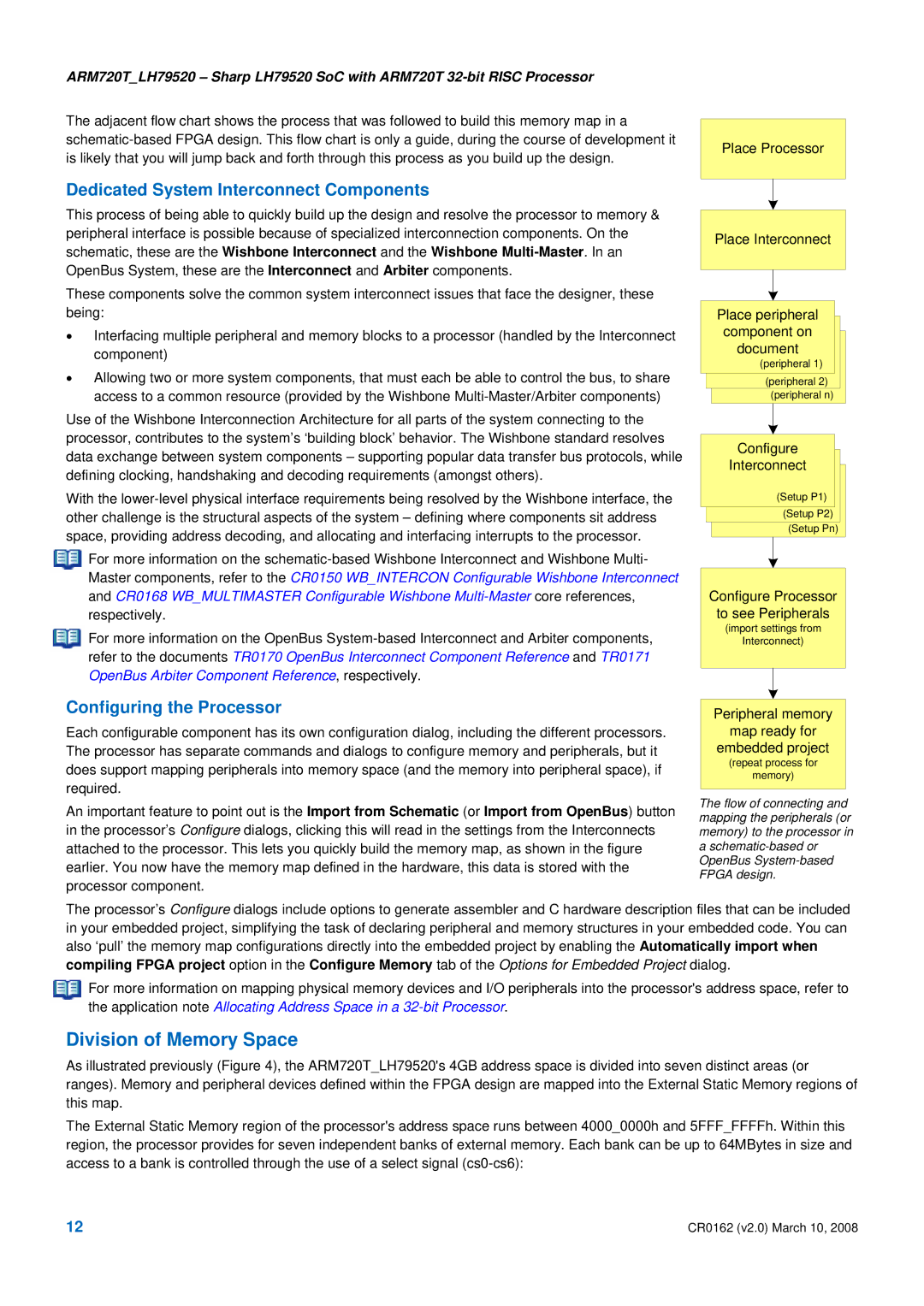
The adjacent flow chart shows the process that was followed to build this memory map in a
Place Processor
Dedicated System Interconnect Components
This process of being able to quickly build up the design and resolve the processor to memory & peripheral interface is possible because of specialized interconnection components. On the schematic, these are the Wishbone Interconnect and the Wishbone
These components solve the common system interconnect issues that face the designer, these being:
•Interfacing multiple peripheral and memory blocks to a processor (handled by the Interconnect component)
•Allowing two or more system components, that must each be able to control the bus, to share access to a common resource (provided by the Wishbone
Use of the Wishbone Interconnection Architecture for all parts of the system connecting to the processor, contributes to the system’s ‘building block’ behavior. The Wishbone standard resolves data exchange between system components – supporting popular data transfer bus protocols, while defining clocking, handshaking and decoding requirements (amongst others).
With the
For more information on the
For more information on the OpenBus
Place Interconnect
Place peripheral component on document
(peripheral 1)
(peripheral 2)
(peripheral n)
Configure
Interconnect
(Setup P1)
(Setup P2)
(Setup Pn)
Configure Processor
to see Peripherals
(import settings from
Interconnect)
Configuring the Processor
Each configurable component has its own configuration dialog, including the different processors. The processor has separate commands and dialogs to configure memory and peripherals, but it does support mapping peripherals into memory space (and the memory into peripheral space), if required.
An important feature to point out is the Import from Schematic (or Import from OpenBus) button in the processor’s Configure dialogs, clicking this will read in the settings from the Interconnects attached to the processor. This lets you quickly build the memory map, as shown in the figure earlier. You now have the memory map defined in the hardware, this data is stored with the processor component.
Peripheral memory
map ready for
embedded project
(repeat process for
memory)
The flow of connecting and mapping the peripherals (or memory) to the processor in
a
The processor’s Configure dialogs include options to generate assembler and C hardware description files that can be included in your embedded project, simplifying the task of declaring peripheral and memory structures in your embedded code. You can also ‘pull’ the memory map configurations directly into the embedded project by enabling the Automatically import when compiling FPGA project option in the Configure Memory tab of the Options for Embedded Project dialog.
For more information on mapping physical memory devices and I/O peripherals into the processor's address space, refer to the application note Allocating Address Space in a
Division of Memory Space
As illustrated previously (Figure 4), the ARM720T_LH79520's 4GB address space is divided into seven distinct areas (or ranges). Memory and peripheral devices defined within the FPGA design are mapped into the External Static Memory regions of this map.
The External Static Memory region of the processor's address space runs between 4000_0000h and 5FFF_FFFFh. Within this region, the processor provides for seven independent banks of external memory. Each bank can be up to 64MBytes in size and access to a bank is controlled through the use of a select signal
12 | CR0162 (v2.0) March 10, 2008 |