Application Report
July
SLAA040
TParalInteMS3rflelADConvertertotheacing20C54xDSPtheTLV1562
IMPORTANT NOTICE
Contents
8.5.5
List of Tables
List of Figures
Figures
viSLAA040
2 The Board
Interfacing the TLV1562 Parallel ADC to the TMS320C54x DSP
1 Introduction
2.1 TMS320C54x Starter Kit
2.3.1 Suggestions for the ’C54x to TLV1562 Interface
2.2 TLV1562EVM
2.3 ADC TLV1562 Overview
2.3.1.1 The Universal Interface
2.3.2 Recyclic Architecture
Using RD or the CSTART Signal to Start Conversion
Figure 2. TLV1562 to ’C54x DSP Interface of the EVM
2.4 Onboard Components
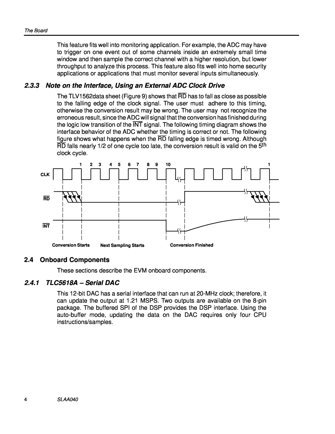
2.3.3 Note on the Interface, Using an External ADC Clock Drive
2.4.1 TLC5618A - Serial DAC
Figure 3. TLC5618A to ’C542 DSP Interface
2.4.2 THS5651 - Parallel Output CommsDAC
Figure 4. THS5651 to C542 DSP Interface
3.1 Reference Voltage Inputs
3 Operational Overview
3.2 Input Data Bits
Table 1. Signal Connections
3.3 Connections Between the DSP and the EVM
Table 3. 2-Position Jumpers
3.3.1 Jumpers Used on the TLV1562EVM
Table 2. 3-Position Jumpers
8SLAA040
4 The Serial DAC/DSP System
Table 4. DSP/DAC Interconnection
Table 5. DSP Serial Port Signals and Registers
5 The DSP Serial Port
6 Other DSP/TLV1562 Signals
6.1 DSP Internal Serial Port Operation
7.1 Writing to the ADC
7.2 Mono Interrupt Driven Mode Using RD
7 Conversation Between the TLV1562 and the DSP
Table 6. DSP Algorithm for Writing to the ADC
tDCSL-sample+1ADCSYSCLK
Table 7. DSP Algorithm for Mono Interrupt Driven Mode Using RD
tENDATAOUT = 41 ns
Table 8. DSP Algorithm for Mono Interrupt Driven Mode Using CSTART
7.3 Mono Interrupt Driven Mode Using CSTART
14 SLAA040
7.4 Dual Interrupt Driven Mode
Table 9. DSP Algorithm for Dual Interrupt Driven Mode
Table 10. DSP Algorithm for Mono Continuous Mode
7.5 Mono Continuous Mode
16 SLAA040
7.6 Dual Continuous Mode
Table 11. DSP Algorithm for Dual Continuous Mode
8.1 Software Development tools
8 Software Overview
8.2 DSP Memory Map
Figure 5. Memory Map
8.3.1 Optimizing CPU Resources for Maximum Data Rates
8.3.3 Timer Output
8.3 Programming Strategies for the ’C54x, Explanations
8.3.2 Address and Data Bus for I/O Tasks
8.3.4 Data Page Pointer
8.3.5 Generating the Chip Select Signal and the CSTART Signal
8.3.6 Interfacing the Serial DAC 5618A to the DSP
GOTO MARK
8.3.7 Interrupt Latency
8.3.8 Branch Optimization goto/dgoto, call/dcall
MARK DP = #1 ARP = #5
8.4 Software Code Explanation
8.3.9 Enabling Software Modules .if/.elseif/.endif
8.4.1 Software Principals of the Interface
Advantage
8.4.1.2 Timed Solution
8.4.1.1 Software Polling
Disadvantage
Advantages
8.4.1.3 Interrupt Driven Solution
8.4.1.5 Setting the Right Switches
Disadvantages
Task
Table 12. Switch Settings
Table 13. Instruction in the Program Header Step
Table 14. Instruction in the Program Header Step
8.5 Flow Charts and Comments for All Software Modes
8.5.1 The Mono Interrupt Driven Mode Using RD to Start Conversion
8.4.1.6 Common Software for all Modes
Code verification
Program Files
Other Files
common file of all modes constants definition
Figure 6. Software Flow of the Mono Interrupt Driven Solution
Includes the complete software algorithm to control the monomode
8.5.2 Mono Interrupt Driven Mode Using CSTART to Start Conversion
Calibration procedure of the DAC
Common file of all modes constants definition
Poll INTO Pin Until h/0 Transition Occurs
Initialize SPI
SAVE
Pull Down CSTART
8.5.2.1 Throughput Optimization†
This only works for one TLV1562 not multiple because CS is not used
Figure 8. Time Optimization monocst1
8.5.3 Dual Interrupt Driven Mode
Maximum Performance at 1.2 MSPS with Internal Clock
IMPORTANT NOTE The code has been optimized to maximize the data throughput. It was found that CSTART can be pulled low earlier than the data read instruction is performed by the DSP. This saves the 100-ns wait time in STEP 3 because the data read requires at least 100 ns. Therefore, CSTART gets pulled high directly after data read, and the interface becomes faster and gains throughput. This variation will be found in the code. The data acquisition is done in a small number of steps that explains everything inside the code
Software Overview
8.5.4 Mono Continuous Mode
Figure 10. Flow Chart Mono Continuous Mode
8.5.5 Dual Continuous Mode
Figure 11. Flow Chart Dual Continuous Mode
Other Files
8.6.1 Common Software for all Modes except C-Callable
8.6 Source Code
8.6.1.1 Constants.asm
set 000C0h Operate without calibrated inputs no offset
42 SLAA040
8.6.1.2 Interrupt Vectors
4C internal timer interrupt
44 SLAA040
File Linker.lnk COMMAND FILE
8.6.1.3 linker,cmd
8.6.1.4 Auto.bat
title ”COMMAND FILE FOR TLV1562.ASM”
jump address to init. new channel
Mainprogram Monomode.asm
pointer address when using any of the following variables
counter for one channel
sent value to register CR0 of the ADC
endif if INT0DRIVENPOLLINGDRV
if SENDOUTSERIAL
48 SLAA040
endif
= bit*AR5,15-0
if AUTOPWDNENABLE
endif if DIFFINPUTMODE
elseif INT0DRIVEN
elseif NOINT0SIG
52 SLAA040
8.6.3 Calibration of the ADC
CALIBRAT.ASM
54 SLAA040
if SMECALIBRATION
56 SLAA040
endif
58 SLAA040
Software Overview
60 SLAA040
if INT0DRIVENPOLLINGDRV
62 SLAA040
= bit*AR5,15-0
endif if SAVEINTOMEMORY
64 SLAA040
endif
Interrupt Routine handler - see 8.6.1.2 Interrupt Vectors
8.6.5 Dual Interrupt Driven Mode
Constants definition - see 8.6.1.1 Constants.asm
Mainprogram DUALIRQ1.asm
Software Overview
Interfacing the TLV1562 Parallel ADC to the TMS320C54x DSP
Software Overview
if SENDOUTSERIAL
endif
70 SLAA040
endif
72 SLAA040
if SAVEINTOMEMORY
Mainprogram MONOCON1.asm
8.6.6 Mono Continuous Mode
74 SLAA040
Software Overview
76 SLAA040
endif if EXTERNALCLOCK
78 SLAA040
endif
Mainprogram DUALCON1.asm
8.6.7 Dual Continuous Mode
80 SLAA040
Software Overview
82 SLAA040
endif if DIFFINPUTMODE
84 SLAA040
Software Overview
TLV1562Channel, Save Memory Start address, NUMBEROFSAMPLES
8.6.8 C-Callable
Mainprogram C1562.c
80h samples of channel 1 will be stored beginning on 2000h
Software Overview
88 SLAA040
AR7+ = data@ADSAMPLE
Vectors.asm
90 SLAA040
int2 returnenable 48 external interrupt int2 nop
Linker.cmd
Auto.bat
92 SLAA040
9 Summary
10 References