Overview
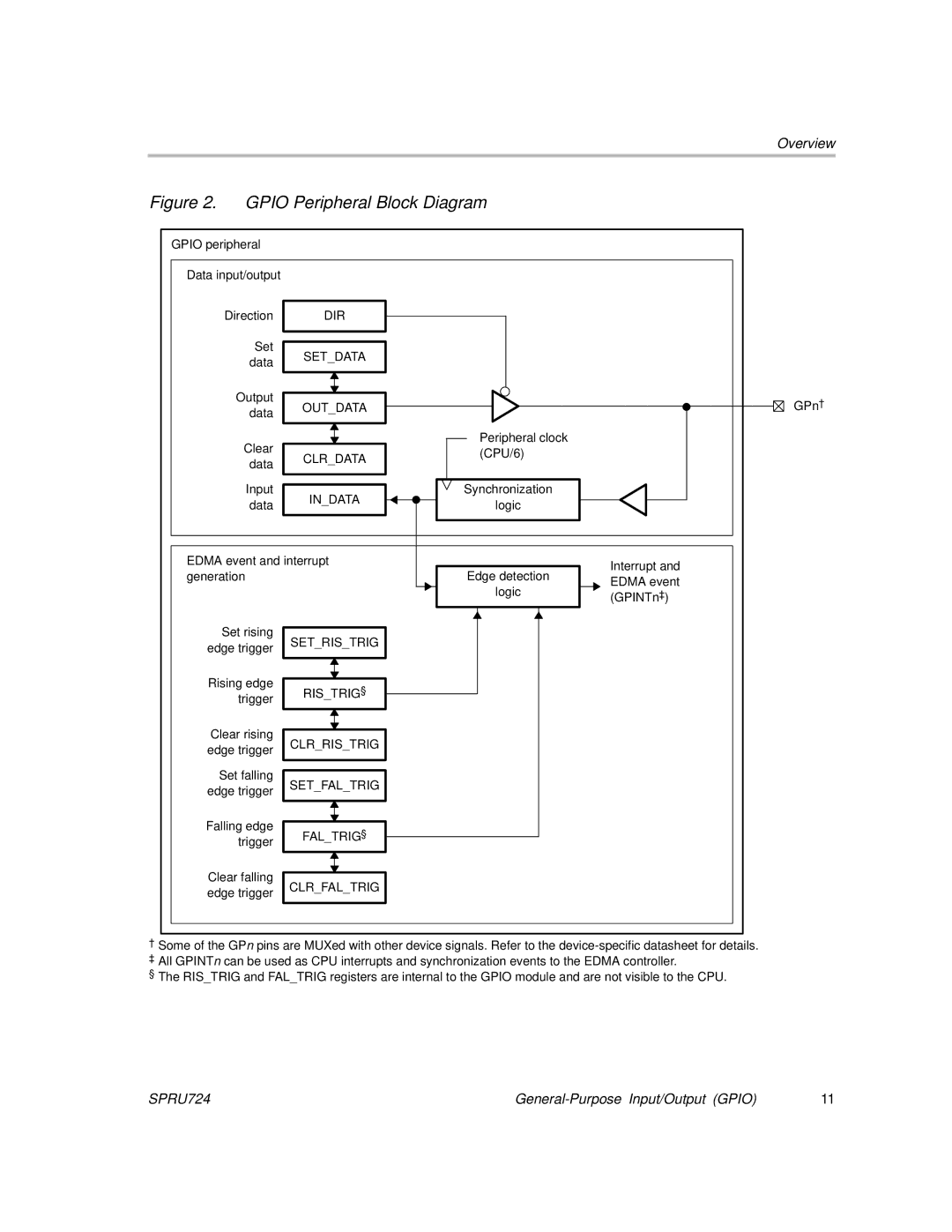
Figure 2. GPIO Peripheral Block Diagram
GPIO peripheral
Data input/output
Direction
Set data
Output data
Clear
data
Input
data
DIR
SET_DATA
OUT_DATA
CLR_DATA
IN_DATA
Peripheral clock (CPU/6)
Synchronization
logic
GPn†
EDMA event and interrupt |
|
| Interrupt and | |||
generation |
|
|
| Edge detection |
| |
|
|
|
| EDMA event | ||
|
|
|
| logic |
| |
|
|
|
|
| (GPINTn‡) | |
Set rising |
|
|
|
|
|
|
SET_RIS_TRIG |
|
|
|
|
| |
edge trigger |
|
|
|
| ||
|
|
|
|
|
| |
|
|
|
|
|
|
|
Rising edge trigger
Clear rising edge trigger
Set falling edge trigger
Falling edge trigger
Clear falling edge trigger
RIS_TRIG§
CLR_RIS_TRIG
SET_FAL_TRIG
FAL_TRIG§
CLR_FAL_TRIG
†Some of the GPn pins are MUXed with other device signals. Refer to the
‡ All GPINTn can be used as CPU interrupts and synchronization events to the EDMA controller.
§ The RIS_TRIG and FAL_TRIG registers are internal to the GPIO module and are not visible to the CPU.
SPRU724 | 11 |