Registers
5.3Output Data Register (OUT_DATA)
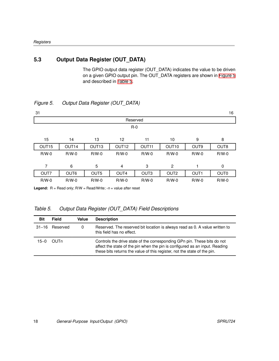
The GPIO output data register (OUT_DATA) indicates the value to be driven on a given GPIO output pin. The OUT_DATA registers are shown in Figure 5 and described in Table 5.
Figure 5. | Output Data Register (OUT_DATA) |
|
|
|
| |||
31 |
|
|
|
|
|
|
| 16 |
|
|
|
|
|
|
|
| |
|
|
| Reserved |
|
|
| ||
|
|
|
|
|
|
|
|
|
|
|
|
|
|
|
| ||
15 | 14 | 13 | 12 |
| 11 | 10 | 9 | 8 |
|
|
|
|
|
|
|
|
|
OUT15 | OUT14 | OUT13 | OUT12 |
| OUT11 | OUT10 | OUT9 | OUT8 |
|
|
|
|
|
|
|
|
|
7 | 6 | 5 | 4 |
| 3 | 2 | 1 | 0 |
|
|
|
|
|
|
|
| |
OUT7 | OUT6 | OUT5 | OUT4 |
| OUT3 | OUT2 | OUT1 | OUT0 |
|
|
|
|
|
|
|
|
|
Legend: R = Read only; R/W = Read/Write; |
|
|
|
| ||||
Table 5. | Output Data Register (OUT_DATA) Field Descriptions | ||
|
|
|
|
Bit | Field | Value | Description |
|
|
|
|
31−16 | Reserved | 0 | Reserved. The reserved bit location is always read as 0. A value written to |
|
|
| this field has no effect. |
|
|
|
|
15−0 | OUTn |
| Controls the drive state of the corresponding GPn pin. These bits do not |
|
|
| affect the state of the pin when the pin is configured as an input. Reading |
|
|
| these bits returns the value of this register, not the state of the pin. |
|
|
|
|
18 | SPRU724 |