Overview
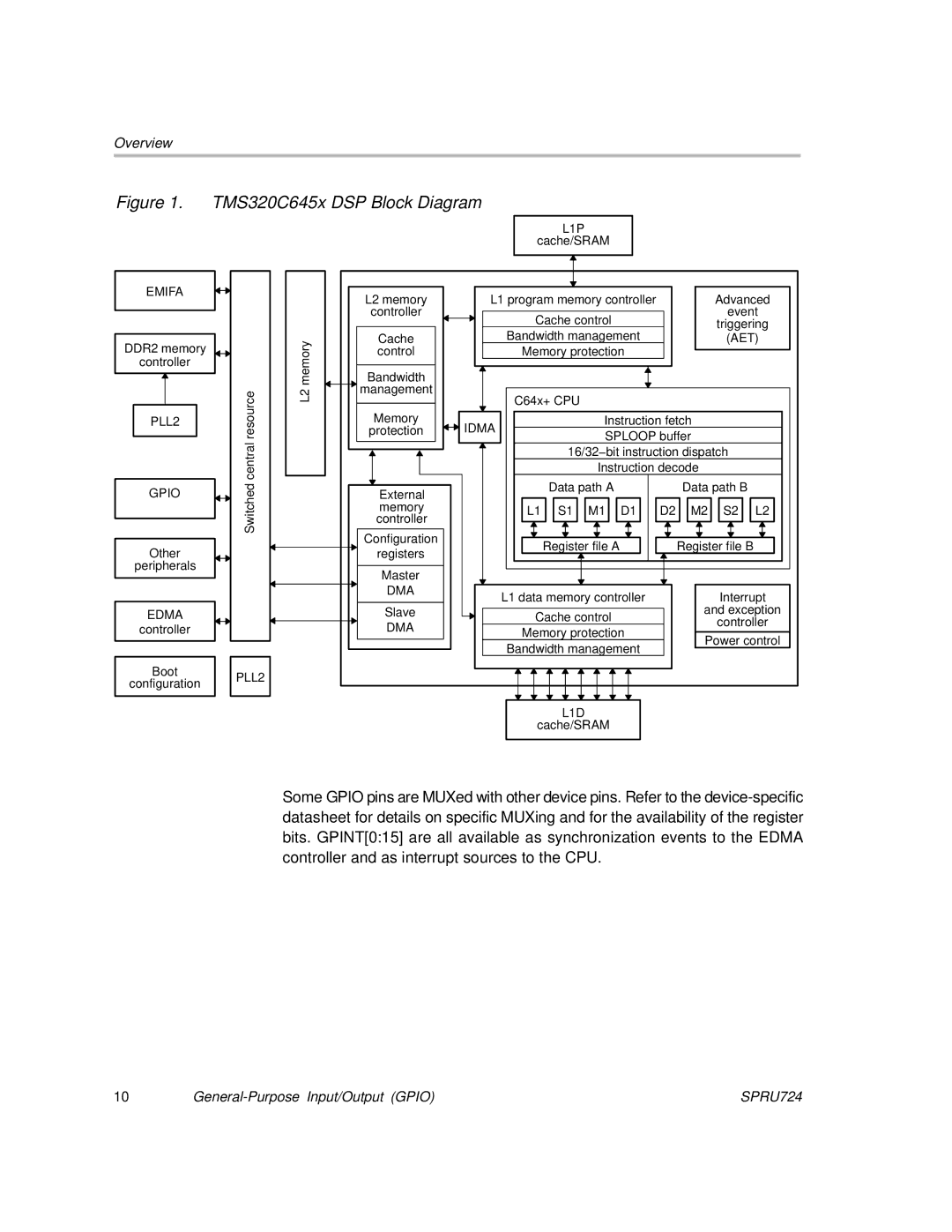
Figure 1. TMS320C645x DSP Block Diagram
EMIFA
DDR2 memory
controller
PLL2
GPIO
Other peripherals
EDMA
controller
Boot
configuration
|
|
|
| L1P |
|
|
|
|
|
|
|
|
| cache/SRAM |
|
|
|
|
| ||
|
| L2 memory | L1 program memory controller |
|
| Advanced | ||||
|
| controller | Cache control |
|
|
| event | |||
|
|
|
|
|
| triggering | ||||
|
|
| Bandwidth management |
|
| |||||
| memory | Cache |
|
| (AET) | |||||
| control | Memory protection |
|
|
|
| ||||
| Bandwidth |
|
|
|
|
|
|
|
| |
resource | L2 | management | C64x+ CPU |
|
|
|
|
|
| |
|
|
|
|
|
|
| ||||
Memory | IDMA |
| Instruction fetch |
|
| |||||
protection |
| SPLOOP buffer |
|
| ||||||
central |
|
|
|
|
|
| ||||
|
|
| 16/32−bit instruction dispatch |
| ||||||
|
|
|
| Instruction decode |
|
| ||||
|
|
| Data path A |
|
| Data path B |
| |||
Switched |
| External |
|
|
|
| ||||
|
|
|
|
|
|
|
|
| ||
| memory | L1 | S1 | M1 | D1 | D2 | M2 | S2 | L2 | |
| controller | |||||||||
|
|
|
|
|
|
|
|
| ||
| Configuration |
|
|
|
|
|
|
|
| |
|
|
| Register file A |
|
| Register file B |
| |||
|
| registers |
|
|
|
| ||||
|
|
|
|
|
|
|
|
|
| |
|
| Master |
|
|
|
|
|
|
|
|
|
| DMA | L1 data memory controller |
|
| Interrupt | ||||
|
|
|
|
| ||||||
|
| Slave | Cache control |
|
| and exception | ||||
|
| DMA |
|
|
| controller | ||||
|
| Memory protection |
|
| ||||||
|
|
| Power control | |||||||
|
|
|
| |||||||
|
|
| Bandwidth management |
| ||||||
|
|
|
|
|
|
| ||||
PLL2 |
|
|
|
|
|
|
|
|
|
|
|
|
|
| L1D |
|
|
|
|
|
|
|
|
| cache/SRAM |
|
|
|
|
| ||
Some GPIO pins are MUXed with other device pins. Refer to the
10 | SPRU724 |