AM64/128A User Manual | Appendix A - Interface Connections |
|
|
APPENDIX A - Interface Pin Connections
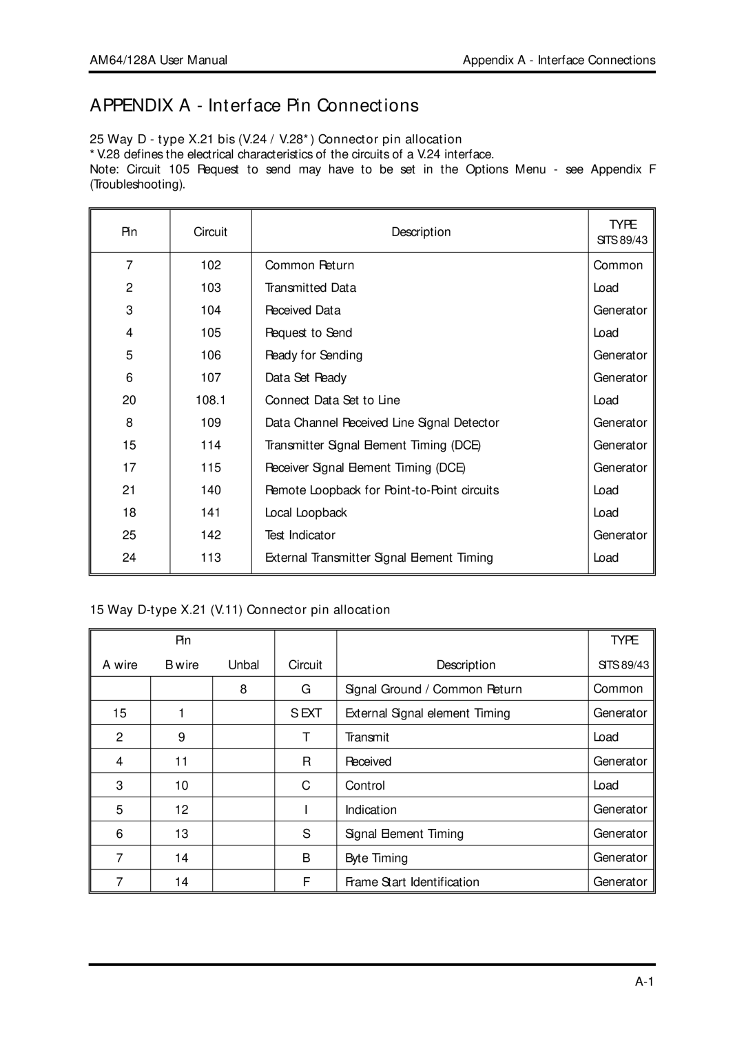
25 Way D - type X.21 bis (V.24 / V.28*) Connector pin allocation
*V.28 defines the electrical characteristics of the circuits of a V.24 interface.
Note: Circuit 105 Request to send may have to be set in the Options Menu - see Appendix F (Troubleshooting).
Pin | Circuit | Description | TYPE | |
SITS 89/43 | ||||
|
|
| ||
|
|
|
| |
7 | 102 | Common Return | Common | |
2 | 103 | Transmitted Data | Load | |
3 | 104 | Received Data | Generator | |
4 | 105 | Request to Send | Load | |
5 | 106 | Ready for Sending | Generator | |
6 | 107 | Data Set Ready | Generator | |
20 | 108.1 | Connect Data Set to Line | Load | |
8 | 109 | Data Channel Received Line Signal Detector | Generator | |
15 | 114 | Transmitter Signal Element Timing (DCE) | Generator | |
17 | 115 | Receiver Signal Element Timing (DCE) | Generator | |
21 | 140 | Remote Loopback for | Load | |
18 | 141 | Local Loopback | Load | |
25 | 142 | Test Indicator | Generator | |
24 | 113 | External Transmitter Signal Element Timing | Load | |
|
|
|
| |
|
|
|
|
15 Way D-type X.21 (V.11) Connector pin allocation
| Pin |
|
|
| TYPE |
A wire | B wire | Unbal | Circuit | Description | SITS 89/43 |
|
|
|
|
|
|
|
| 8 | G | Signal Ground / Common Return | Common |
|
|
|
|
|
|
15 | 1 |
| S EXT | External Signal element Timing | Generator |
|
|
|
|
|
|
2 | 9 |
| T | Transmit | Load |
|
|
|
|
|
|
4 | 11 |
| R | Received | Generator |
|
|
|
|
|
|
3 | 10 |
| C | Control | Load |
|
|
|
|
|
|
5 | 12 |
| I | Indication | Generator |
|
|
|
|
|
|
6 | 13 |
| S | Signal Element Timing | Generator |
|
|
|
|
|
|
7 | 14 |
| B | Byte Timing | Generator |
|
|
|
|
|
|
7 | 14 |
| F | Frame Start Identification | Generator |
|
|
|
|
|
|
|
|
|
|
|
|
