ADSP-21020
1⋅
CLOCK
![]() 4
4
|
| 2 | CLKIN | RESET | 4 | ||||
SELECTS |
|
|
|
| |||||
|
|
|
|
|
| ||||
PROGRAM | OE |
| PMRD |
|
|
|
| DMRD |
|
WE |
|
|
|
|
|
|
|
| |
MEMORY | 24 | PMWR |
|
|
|
| DMWR | 32 | |
| ADDR | PMA |
|
|
|
| DMA | ||
| 48 |
|
|
|
| 32 | |||
| DATA | PMD |
|
|
|
| DMD | ||
|
|
|
|
|
|
| |||
|
|
|
|
| |||||
|
|
|
| ||||||
|
|
| PMTS |
|
|
|
| DMTS |
|
|
|
| PMPAGE |
|
| DMPAGE |
| ||
|
|
| PMACK |
|
|
|
| DMACK |
|
|
|
| BR | BG | TIMEXP | RCOMP | JTAG |
| |
|
|
|
|
|
|
|
|
|
|
|
|
|
|
|
| 4 |
| 5 |
|
SELECTS |
| |
OE | DATA | |
WE | ||
MEMORY | ||
ADDR | ||
| ||
DATA |
| |
|
|
![]() SELECTS
SELECTS
![]() OE
OE
PERIPHERALS
WE ACK
![]() ADDR
ADDR ![]() DATA
DATA
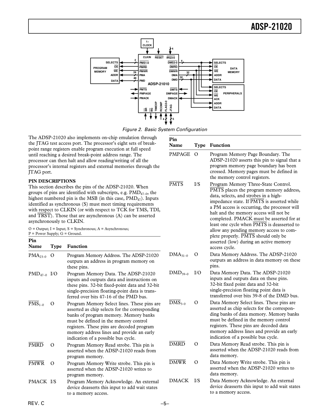
Figure 2. Basic System Configuration
The
PIN DESCRIPTIONS
This section describes the pins of the ADSP-21020. When
groups of pins are identified with subscripts, e.g.
identified as synchronous (S) must meet timing requirements with respect to CLKIN (or with respect to TCK for TMS, TDI, and TRST). Those that are asynchronous (A) can be asserted asynchronously to CLKIN.
O = Output; I = Input; S = Synchronous; A = Asynchronous; P = Power Supply; G = Ground.
Pin
Name Type Function
| O | Program Memory Address. The | ||||
|
|
|
|
|
| outputs an address in program memory on |
|
|
|
|
|
| these pins. |
| I/O | Program Memory Data. The | ||||
|
|
|
|
|
| inputs and outputs data and instructions on |
|
|
|
|
|
| these pins. |
|
|
|
|
|
| |
|
|
|
|
|
| ferred over bits |
|
| O | Program Memory Select lines. These pins are | |||
| PMS | |||||
|
|
|
|
|
| asserted as chip selects for the corresponding |
|
|
|
|
|
| banks of program memory. Memory banks |
|
|
|
|
|
| must be defined in the memory control |
|
|
|
|
|
| registers. These pins are decoded program |
|
|
|
|
|
| memory address lines and provide an early |
|
|
|
|
|
| indication of a possible bus cycle. |
|
|
|
| O | Program Memory Read strobe. This pin is | |
| PMRD | |||||
|
|
|
|
|
| asserted when the |
|
|
|
|
|
| program memory. |
|
|
| O | Program Memory Write strobe. This pin is | ||
| PMWR | |||||
|
|
|
|
|
| asserted when the |
|
|
|
|
|
| program memory. |
| PMACK | I/S | Program Memory Acknowledge. An external | |||
|
|
|
|
|
| device deasserts this input to add wait states |
|
|
|
|
|
| to a memory access. |
REV. C |
|
| ||||
Pin |
|
|
|
|
|
|
|
|
| ||||
Name | Type | Function | |||||||||||
|
|
|
|
|
|
|
|
|
|
|
|
|
|
PMPAGE | O | Program Memory Page Boundary. The | |||||||||||
|
|
|
|
|
| ||||||||
|
|
|
|
|
| program memory page boundary has been | |||||||
|
|
|
|
|
| crossed. Memory pages must be defined in | |||||||
|
|
|
|
|
| the memory control registers. | |||||||
|
|
|
|
| I/S | Program Memory | |||||||
PMTS | |||||||||||||
|
|
|
|
|
| PMTS | places the program memory address, | ||||||
|
|
|
|
|
| data, selects, and strobes in a high- | |||||||
|
|
|
|
|
| impedance state. If | PMTS | is asserted while | |||||
|
|
|
|
|
| a PM access is occurring, the processor will | |||||||
|
|
|
|
|
| halt and the memory access will not be | |||||||
|
|
|
|
|
| completed. PMACK must be asserted for at | |||||||
|
|
|
|
|
| least one cycle when | PMTS | is deasserted to | |||||
|
|
|
|
|
| allow any pending memory access to com- | |||||||
|
|
|
|
|
| plete properly. | PMTS | should only be | |||||
|
|
|
|
|
| asserted (low) during an active memory | |||||||
|
|
|
|
|
| access cycle. | |||||||
O | Data Memory Address. The | ||||||||||||
|
|
|
|
|
| outputs an address in data memory on these | |||||||
|
|
|
|
|
| pins. | |||||||
I/O | Data Memory Data. The | ||||||||||||
|
|
|
|
|
| inputs and outputs data on these pins. | |||||||
|
|
|
|
|
| ||||||||
|
|
|
|
|
| ||||||||
|
|
|
|
|
| transferred over bits | |||||||
| O | Data Memory Select lines. These pins are | |||||||||||
DMS | |||||||||||||
|
|
|
|
|
| asserted as chip selects for the correspon- | |||||||
|
|
|
|
|
| ding banks of data memory. Memory banks | |||||||
|
|
|
|
|
| must be defined in the memory control | |||||||
|
|
|
|
|
| registers. These pins are decoded data | |||||||
|
|
|
|
|
| memory address lines and provide an early | |||||||
|
|
|
|
|
| indication of a possible bus cycle. | |||||||
|
|
| O | Data Memory Read strobe. This pin is | |||||||||
DMRD | |||||||||||||
|
|
|
|
|
| asserted when the | |||||||
|
|
|
|
|
| data memory. | |||||||
|
| O | Data Memory Write strobe. This pin is | ||||||||||
DMWR | |||||||||||||
|
|
|
|
|
| asserted when the | |||||||
|
|
|
|
|
| data memory. | |||||||
DMACK | I/S | Data Memory Acknowledge. An external | |||||||||||
|
|
|
|
|
| device deasserts this input to add wait states | |||||||
|
|
|
|
|
| to a memory access. | |||||||