ADSP-21020
TEST CONDITIONS
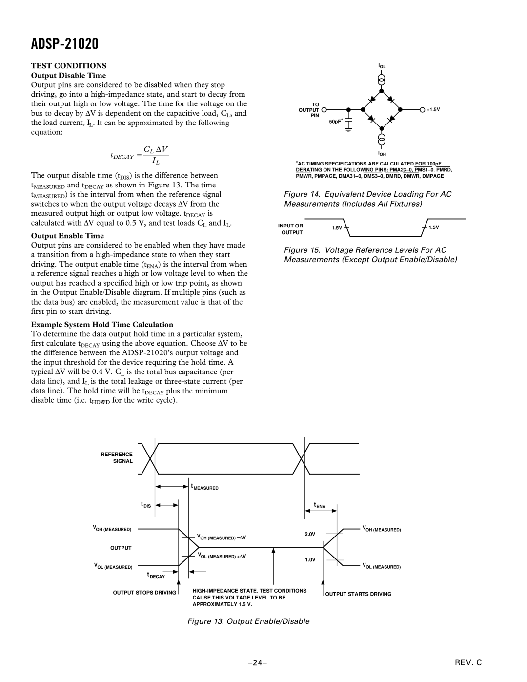
Output Disable Time
Output pins are considered to be disabled when they stop driving, go into a
tDECAY = CL ΔV
IL
The output disable time (tDIS) is the difference between
tMEASURED and tDECAY as shown in Figure 13. The time tMEASURED) is the interval from when the reference signal switches to when the output voltage decays ΔV from the
measured output high or output low voltage. tDECAY is calculated with ΔV equal to 0.5 V, and test loads CL and IL.
Output Enable Time
Output pins are considered to be enabled when they have made a transition from a
Example System Hold Time Calculation
To determine the data output hold time in a particular system,
first calculate tDECAY using the above equation. Choose ΔV to be the difference between the
the input threshold for the device requiring the hold time. A typical ΔV will be 0.4 V. CL is the total bus capacitance (per data line), and IL is the total leakage or
data line). The hold time will be tDECAY plus the minimum disable time (i.e. tHDWD for the write cycle).
IOL
TO
OUTPUT ![]()
![]()
![]()
![]()
![]() +1.5V PIN
+1.5V PIN
50pF* ![]()
IOH
*AC TIMING SPECIFICATIONS ARE CALCULATED FOR 100pF DERATING ON THE FOLLOWING PINS:
PMWR, PMPAGE,
Figure 14. Equivalent Device Loading For AC Measurements (Includes All Fixtures)
INPUT OR | 1.5V | 1.5V |
|
OUTPUT
Figure 15. Voltage Reference Levels For AC Measurements (Except Output Enable/Disable)
REFERENCE |
|
|
SIGNAL |
|
|
| t MEASURED |
|
t DIS |
| tENA |
VOH (MEASURED) |
| VOH (MEASURED) |
| VOH (MEASURED) | 2.0V |
|
| |
OUTPUT |
|
|
| VOL (MEASURED) +ΔV | 1.0V |
VOL (MEASURED) |
| VOL (MEASURED) |
tDECAY
OUTPUT STOPS DRIVING | OUTPUT STARTS DRIVING | ||
CAUSE THIS VOLTAGE LEVEL TO BE | |||
|
| ||
| APPROXIMATELY 1.5 V. |
|
Figure 13. Output Enable/Disable
REV. C |