ADSP-21020
External Memory
|
|
|
|
|
|
| K/B/T Grade | K/B/T Grade | B/T Grade | K Grade |
|
|
| ||||
|
|
|
|
|
|
|
|
|
|
|
|
| |||||
|
|
|
|
|
|
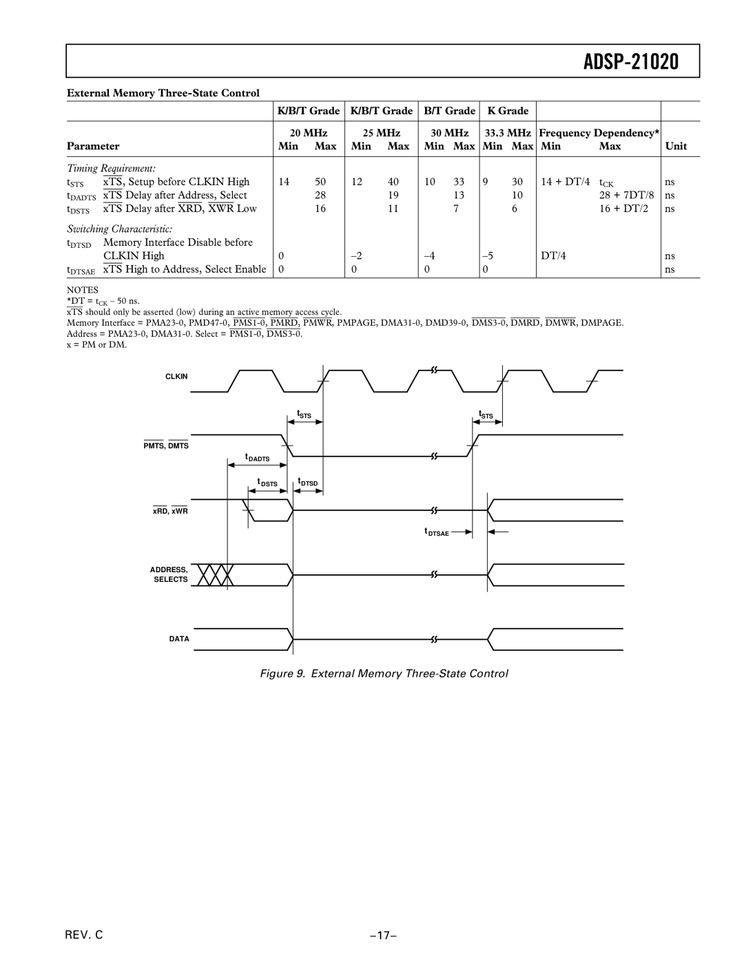
| 20 MHz | 25 MHz | 30 MHz | 33.3 MHz | Frequency Dependency* |
| |||||
Parameter | Min | Max | Min | Max | Min | Max | Min | Max | Min | Max | Unit | ||||||
|
|
|
|
|
|
|
|
|
|
|
|
|
|
|
|
| |
Timing Requirement: |
|
|
|
|
|
|
|
|
|
|
| ||||||
tSTS |
| , Setup before CLKIN High | 14 | 50 | 12 | 40 | 10 | 33 | 9 | 30 | 14 + DT/4 | tCK | ns | ||||
xTS | |||||||||||||||||
tDADTS | xTS | Delay after Address, Select |
| 28 |
| 19 |
| 13 |
| 10 |
| 28 + 7DT/8 | ns | ||||
tDSTS | xTS | Delay after | XRD | , | XWR | Low |
| 16 |
| 11 |
| 7 |
| 6 |
| 16 + DT/2 | ns |
Switching Characteristic: |
|
|
|
|
|
|
|
|
|
|
| ||||||
tDTSD | Memory Interface Disable before |
|
|
|
|
|
|
|
|
|
|
| |||||
| CLKIN High | 0 |
|
|
|
| DT/4 |
| ns | ||||||||
tDTSAE |
| High to Address, Select Enable | 0 |
| 0 |
| 0 |
| 0 |
|
|
| ns | ||||
xTS |
|
|
|
|
|
| |||||||||||
NOTES
*DT = tCK – 50 ns.
xTS should only be asserted (low) during an active memory access cycle.
Memory Interface =
x = PM or DM.
CLKIN
tSTS | tSTS |
PMTS, DMTS
tDADTS
t DSTS | tDTSD |
xRD, xWR
t DTSAE ![]()
ADDRESS,
SELECTS
DATA
Figure 9. External Memory Three-State Control
REV. C |