ADSP-21020
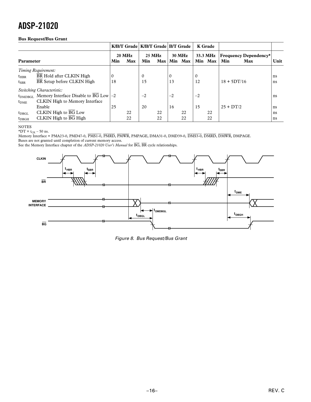
Bus Request/Bus Grant
|
|
|
|
|
|
| K/B/T Grade | K/B/T Grade | B/T Grade | K Grade |
|
|
|
|
|
|
|
|
|
|
|
|
|
|
|
| |
|
|
|
|
|
|
| 20 MHz | 25 MHz | 30 MHz | 33.3 MHz | Frequency Dependency* |
| |
Parameter | Min Max | Min Max | Min Max | Min Max | Min | Max | Unit | ||||||
|
|
|
|
|
|
|
|
|
|
|
|
| |
Timing Requirement: |
|
|
|
|
|
|
| ||||||
tHBR |
| Hold after CLKIN High | 0 | 0 | 0 | 0 |
|
| ns | ||||
BR |
|
| |||||||||||
tSBR | BR | Setup before CLKIN High | 18 | 15 | 13 | 12 | 18 + 5DT/16 | ns | |||||
Switching Characteristic: |
|
|
|
|
|
|
| ||||||
tDMDBGL | Memory Interface Disable to |
| Low |
|
| ns | |||||||
BG |
|
| |||||||||||
tDME | CLKIN High to Memory Interface |
|
|
|
|
|
|
| |||||
| Enable | 25 | 20 | 16 | 15 | 25 + DT/2 |
| ns | |||||
tDBGL | CLKIN High to |
| Low | 22 | 22 | 22 | 22 |
|
| ns | |||
BG |
|
| |||||||||||
tDBGH | CLKIN High to | BG | High | 22 | 22 | 22 | 22 |
|
| ns | |||
NOTES
*DT = tCK – 50 ns.
Memory Interface =
See the Memory Interface chapter of the
CLKIN
t HBR | tSBR | t HBR | tSBR |
BR
tDME
MEMORY
INTERFACE
![]() tDMDBGL
tDMDBGL
tDBGL | tDBGH |
BG
Figure 8. Bus Request/Bus Grant
REV. C |
