Capacitive Loading
Output delays are based on standard capacitive loads: 100 pF on address, select, page and strobe pins, and 50 pF on all others (see Figure 14). For different loads, these timing parameters should be derated. See the Hardware Configuration chapter of the
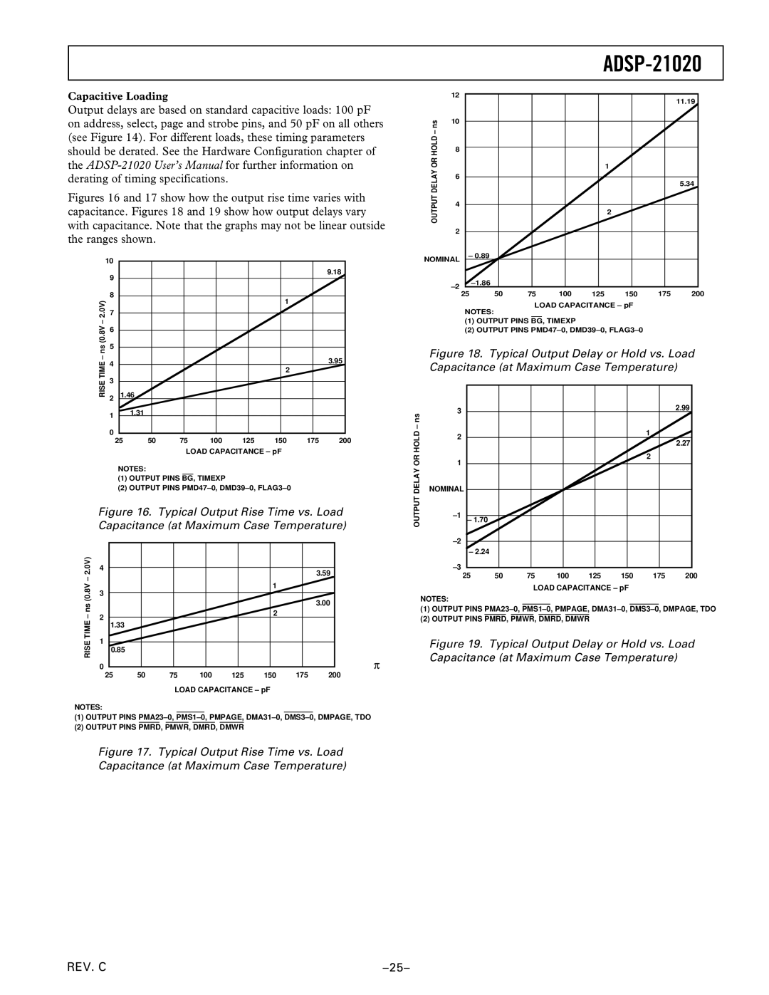
Figures 16 and 17 show how the output rise time varies with capacitance. Figures 18 and 19 show how output delays vary with capacitance. Note that the graphs may not be linear outside the ranges shown.
| 10 |
|
|
|
|
|
|
|
|
|
|
|
|
|
|
|
|
|
|
|
|
| |
|
|
|
|
|
|
|
|
|
|
|
|
| 9 |
|
|
|
|
|
|
|
| 9.18 |
|
|
|
|
|
|
|
|
|
|
|
| |
2.0V) | 8 |
|
|
|
|
|
| 1 |
|
|
|
|
|
|
|
|
|
|
|
|
| ||
7 |
|
|
|
|
|
|
|
|
|
| |
– |
|
|
|
|
|
|
|
|
|
|
|
(0.8V | 6 |
|
|
|
|
|
|
|
|
|
|
|
|
|
|
|
|
|
|
|
|
| |
– ns | 5 |
|
|
|
|
|
|
|
|
|
|
|
|
|
|
|
|
|
|
| 3.95 |
| |
TIME | 4 |
|
|
|
|
|
|
|
|
| |
|
|
|
|
|
| 2 |
|
|
| ||
|
|
|
|
|
|
|
|
|
| ||
|
|
|
|
|
|
|
|
|
|
| |
RISE | 3 |
|
|
|
|
|
|
|
|
|
|
2 |
| 1.46 |
|
|
|
|
|
|
|
| |
|
|
|
|
|
|
|
|
|
|
| |
| 1 |
| 1.31 |
|
|
|
|
|
|
|
|
|
|
|
|
|
|
|
|
|
|
| |
| 0 |
|
|
|
|
|
|
|
|
|
|
| 25 | 50 | 75 | 100 | 125 | 150 | 175 | 200 | |||
|
| ||||||||||
|
|
|
|
| LOAD CAPACITANCE – pF |
|
|
| |||
NOTES:
(1)OUTPUT PINS BG, TIMEXP
(2)OUTPUT PINS
Figure 16. Typical Output Rise Time vs. Load Capacitance (at Maximum Case Temperature)
2.0V) | 4 |
|
|
|
|
|
|
| 3.59 |
|
|
|
|
|
|
|
|
|
| ||
– |
|
|
|
|
|
|
|
|
| |
|
|
|
|
|
| 1 |
|
|
| |
(0.8V | 3 |
|
|
|
|
|
|
|
| |
|
|
|
|
|
|
|
|
| ||
|
|
|
|
|
|
|
|
|
| |
– ns |
|
|
|
|
|
|
|
| 3.00 |
|
2 |
|
|
|
|
| 2 |
|
|
| |
TIME | 1.33 |
|
|
|
|
|
|
|
| |
|
|
|
|
|
|
|
|
| ||
|
|
|
|
|
|
|
|
|
| |
RISE | 1 | 0.85 |
|
|
|
|
|
|
|
|
|
|
|
|
|
|
|
|
| ||
|
|
|
|
|
|
|
|
|
| |
| 0 |
|
|
|
|
|
|
|
| π |
|
|
|
|
|
|
|
|
| ||
| 25 | 50 | 75 | 100 | 125 | 150 | 175 | 200 | ||
LOAD CAPACITANCE – pF
NOTES:
(1)OUTPUT PINS
(2)OUTPUT PINS PMRD, PMWR, DMRD, DMWR
Figure 17. Typical Output Rise Time vs. Load Capacitance (at Maximum Case Temperature)
ADSP-21020
| 12 |
|
|
|
|
|
|
|
| 11.19 |
|
|
|
|
|
|
|
|
|
|
|
| |
– ns | 10 |
|
|
|
|
|
|
|
|
|
|
|
|
|
|
|
|
|
|
|
|
| |
HOLDOR | 8 |
|
|
|
|
|
|
|
|
|
|
DELAY |
|
|
|
|
|
|
| 1 |
|
|
|
6 |
|
|
|
|
|
|
|
| 5.34 |
| |
OUTPUT |
|
|
|
|
|
|
|
|
|
| |
4 |
|
|
|
|
|
| 2 |
|
|
| |
|
|
|
|
|
|
|
|
|
| ||
|
|
|
|
|
|
|
|
|
|
| |
| 2 |
|
|
|
|
|
|
|
|
|
|
NOMINAL |
| – 0.89 |
|
|
|
|
|
|
|
| |
|
|
|
|
|
|
|
|
|
| ||
|
|
|
|
|
|
|
|
|
| ||
| 25 | 50 | 75 | 100 | 125 | 150 | 175 | 200 | |||
|
| ||||||||||
LOAD CAPACITANCE – pF
NOTES:
(1)OUTPUT PINS BG, TIMEXP
(2)OUTPUT PINS
Figure 18. Typical Output Delay or Hold vs. Load Capacitance (at Maximum Case Temperature)
– ns | 3 |
|
|
|
|
|
|
| 2.99 |
|
|
|
|
|
|
|
|
|
| ||
|
|
|
|
|
|
| 1 |
|
| |
HOLD | 2 |
|
|
|
|
|
|
|
| |
|
|
|
|
|
|
| 2.27 |
| ||
|
|
|
|
|
|
|
|
| ||
|
|
|
|
|
|
|
|
|
| |
OR | 1 |
|
|
|
|
|
| 2 |
|
|
|
|
|
|
|
|
|
|
| ||
DELAY | NOMINAL |
|
|
|
|
|
|
|
|
|
OUTPUT | – 1.70 |
|
|
|
|
|
|
|
| |
|
|
|
|
|
|
|
|
| ||
|
|
|
|
|
|
|
|
|
| |
|
| – 2.24 |
|
|
|
|
|
|
|
|
|
|
|
|
|
|
|
|
|
| |
|
|
|
|
|
|
|
|
|
| |
| 25 | 50 | 75 | 100 | 125 | 150 | 175 | 200 | ||
LOAD CAPACITANCE – pF
NOTES:
(1)OUTPUT PINS
(2)OUTPUT PINS PMRD, PMWR, DMRD, DMWR
Figure 19. Typical Output Delay or Hold vs. Load Capacitance (at Maximum Case Temperature)
REV. C |