ADSP-21020
TIMING PARAMETERS
General Notes
See Figure 15 on page 24 for voltage reference levels. Use the exact timing information given. Do not attempt to derive parameters from the addition or subtraction of others. While addition or subtraction would yield meaningful results for an individual device, the values given in this data sheet reflect statistical variations and worst cases. Consequently, you cannot meaningfully add parameters to derive other specifications.
Clock Signal
|
| K/B/T Grade |
|
| K/B/T Grade |
|
|
| B/T Grade |
| K Grade |
|
| |||||
|
|
|
|
|
|
|
|
|
|
|
|
|
|
|
| |||
|
|
| 20 MHz |
|
| 25 MHz |
|
|
| 30 MHz |
| 33.3 MHz |
|
| ||||
Parameter | Min | Max |
|
| Min | Max |
|
| Min | Max |
| Min | Max |
| Unit | |||
|
|
|
|
|
|
|
|
|
|
|
|
|
|
|
|
|
| |
Timing Requirement: |
|
|
|
|
|
|
|
|
|
|
|
|
|
|
|
|
| |
tCK | CLKIN Period | 50 | 150 |
|
| 40 | 150 |
|
| 33 | 150 |
| 30 | 150 |
| ns | ||
tCKH | CLKIN Width High | 10 |
|
|
| 10 |
|
|
| 10 |
|
| 10 |
|
| ns | ||
tCKL | CLKIN Width Low | 10 |
|
|
| 10 |
|
|
| 10 |
|
| 10 |
|
| ns | ||
|
|
|
|
|
|
| t CK |
|
|
|
|
|
|
|
|
|
|
|
|
| CLKIN |
|
|
|
|
|
|
|
|
|
|
|
|
|
|
| |
|
|
|
|
|
| t CKH | tCKL |
|
|
|
|
|
|
|
| |||
|
|
|
|
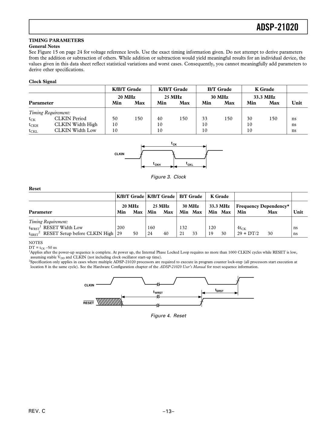
| Figure 3. Clock |
|
|
|
|
|
|
|
|
|
| |||
Reset |
|
|
|
|
|
|
|
|
|
|
|
|
|
|
|
|
|
|
|
|
|
|
|
|
|
|
|
|
|
|
|
| |||||
|
|
| K/B/T Grade | K/B/T Grade | B/T Grade | K Grade |
|
|
|
|
| |||||||
|
|
|
|
|
|
|
|
|
|
|
|
|
| |||||
|
|
| 20 MHz |
| 25 MHz | 30 MHz |
| 33.3 MHz | Frequency Dependency* |
| ||||||||
Parameter |
| Min | Max | Min | Max | Min | Max |
| Min | Max | Min | Max | Unit | |||||
|
|
|
|
|
|
|
|
|
|
|
|
|
|
|
|
|
| |
Timing Requirement: |
|
|
|
|
|
|
|
|
|
|
|
|
|
|
|
|
| |
tWRST1 RESET Width Low |
| 200 |
| 160 |
| 132 |
|
|
| 120 |
| 4tCK |
|
| ns | |||
tSRST2 | RESET Setup before CLKIN High | 29 | 50 | 24 | 40 | 21 | 33 |
| 19 | 30 | 29 + DT/2 | 30 |
| ns | ||||
NOTES
DT = tCK
1Applies after the
2Specification only applies in cases where multiple
CLKIN
tWRST![]() tSRST
tSRST
RESET
Figure 4. Reset
REV. C |