Analog Devices ADSP-21020 manual 3 0.1 inches, Bottom View Ribbon Cable

Models: ADSP-21020

1 32
Download 32 pages 38.92 Kb
Page 27
Image 27

ADSP-21020

All GND pins should have a low impedance path to ground. A ground plane is required in ADSP-21020 systems to reduce this impedance, minimizing noise.

The EVDD and IVDD pins should be bypassed to the ground plane using approximately 14 high-frequency capacitors (0.1 μF ceramic). Keep each capacitor’s lead and trace length to the pins as short as possible. This low inductive path provides the ADSP-21020 with the peak currents required when its output drivers switch. The capacitors’ ground leads should also be short and connect directly to the ground plane. This provides a low impedance return path for the load capacitance of the ADSP-21020’s output drivers.

If a VDD plane is not used, the following recommendations apply. Traces from the +5 V supply to the 10 EVDD pins should be designed to satisfy the minimum VDD specification while carrying average dc currents of [IDDEX/10 3 (number of EVDD pins per trace)]. IDDEX is the calculated external supply current. A similar calculation should be made for the four IVDD pins using the IDDIN specification. The traces connecting +5 V to the IVDD pins should be separate from those con- necting to the EVDD pins.

A low frequency bypass capacitor (20 μF tantalum) located near the junction of the IVDD and EVDD traces is also recommended.

Target System Requirements For Use Of EZ-ICE Emulator

The ADSP-21020 EZ-ICE uses the IEEE 1149.1 JTAG test access port of the ADSP-21020 to monitor and control the target board processor during emulation. The EZ-ICE probe requires that CLKIN, TMS, TCK, TRST, TDI, TDO, and GND be made accessible on the target system via a 12-pin connector (pin strip header) such as that shown in Figure 20. The EZ-ICE probe plugs directly onto this connector for chip-on-board emulation; you must add this connector to your target board design if you intend to use the ADSP-21020 EZ-ICE. Figure 21 shows the dimensions of the EZ-ICE probe; be sure to allow enough space in your system to fit the probe onto the 12-pin connector.

KEY (NO PIN 1)

X

CLKIN

BTMS


TMS

BTCK


TCK

BTRST


TRST

BTDI


TDI

GND


TDO

TOP VIEW

Figure 20. Target Board Connector for EZ-ICE Emulator (Jumpers In Place)
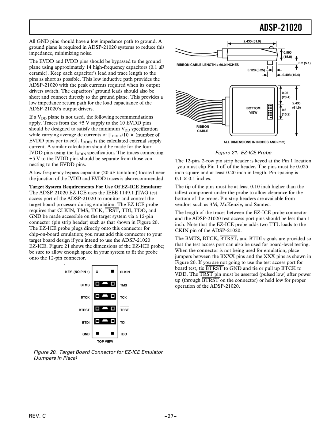
2.435 (61.9)

0.590 (15.0)

RIBBON CABLE LENGTH = 60.0 INCHES

0.128 (3.25)

BOTTOM

VIEW

RIBBON

CABLE

0.2 (5.1)

0.408 (10.4)

0.92

(23.4)

2.435

(61.9)

0.6

(15.2)

ALL DIMENSIONS IN INCHES AND (mm)

Figure 21. EZ-ICE Probe

The 12-pin, 2-row pin strip header is keyed at the Pin 1 location –you must clip Pin 1 off of the header. The pins must be 0.025 inch square and at least 0.20 inch in length. Pin spacing is

0.1 3 0.1 inches.

The tip of the pins must be at least 0.10 inch higher than the tallest component under the probe to allow clearance for the bottom of the probe. Pin strip headers are available from vendors such as 3M, McKenzie, and Samtec.

The length of the traces between the EZ-ICE probe connector and the ADSP-21020 test access port pins should be less than 1 inch. Note that the EZ-ICE probe adds two TTL loads to the CKIN pin of the ADSP-21020.

The BMTS, BTCK, BTRST, and BTDI signals are provided so that the test access port can also be used for board-level testing. When the connector is not being used for emulation, place jumpers between the BXXX pins and the XXX pins as shown in Figure 20. If you are not going to use the test access port for board test, tie BTRST to GND and tie or pull up BTCK to VDD. The TRST pin must be asserted (pulsed low) after power up (through BTRST on the connector) or held low for proper operation of the ADSP-21020.

REV. C

–27–

Page 27
Image 27
Analog Devices ADSP-21020 manual 3 0.1 inches, Bottom View Ribbon Cable