CY14B101K
Real Time Clock Operation
nvTIME Operation
The CY14B101K offers internal registers that contain clock, alarm, watchdog, interrupt, and control functions. RTC registers use the last 16 address locations of the SRAM. Internal double buffering of the clock and the clock or timer information registers prevents accessing transitional internal clock data during a READ or WRITE operation. Double buffering also circumvents disrupting normal timing counts or clock accuracy of the internal clock while accessing clock data. Clock and Alarm Registers store data in BCD format.
The RTC register addresses for CY14B101K range from 0x1FFF0 to 0x1FFFF. Refer to RTC Register Map[5, 6] on page 11 and Register Map Detail on page 12 for detailed description.
Clock Operations
The clock registers maintain time up to 9,999 years in one second increments. The user sets the time to any calendar time and the clock automatically keeps track of days of the week, month, leap years, and century transitions. There are eight registers dedicated to the clock functions that are used to set time with a WRITE cycle and to READ time during a READ cycle. These registers contain the Time of Day in BCD format. Bits defined as ‘0’ are currently not used and are reserved for future use by Cypress.
Reading the Clock
The double buffered RTC register structure reduces the chance of reading incorrect data from the clock. The user should stop internal updates to the CY14B101K time keeping registers before reading clock data, to prevent reading of data in transition. Stopping the internal register updates does not affect clock accuracy.
The updating process is stopped by writing a ‘1’ to the read bit ‘R’ (in the flags register at 0x1FFF0), and does not restart until a ‘0’ is written to the read bit. The RTC registers are then read while the internal clock continues to run. After a ‘0’ is written to the read bit (‘R’), all CY14B101K registers are simultaneously updated within 20 ms.
Setting the Clock
Setting the write bit ‘W’ (in the flags register at 0x1FFF0) to a ‘1’ stops updates to the time keeping registers and enables the time to be set. The correct day, date, and time are then written into the registers in 24 hour BCD format. The time written is referred to as the ‘Base Time’. This value is stored in nonvolatile registers and used in calculation of the current time. Resetting the WRITE bit to ‘0’ transfers those values to the actual clock counters, after which the clock resumes normal operation.
Backup Power
The RTC in the CY14B101K is intended for permanently powered operations. Either the VRTCcap or VRTCbat pin is connected depending on whether a capacitor or battery is chosen for the application. When the primary power, VCC, fails and drops below VSWITCH, the device switches to the backup power supply.
The clock oscillator uses very little current to maximize the backup time available from the backup source. Regardless of clock operation with the primary source removed, the data stored in nvSRAM is secure, as it is stored in the nonvolatile elements when power was lost.
During backup operation, the CY14B101K consumes a maximum of 300 nA at 2V. The user should choose capacitor or battery values according to the application.
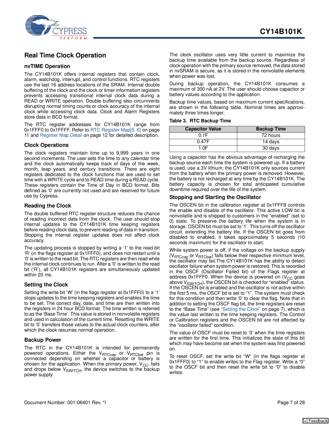
Backup time values, based on maximum current specifications, are shown in the following table. Nominal times are approxi- mately three times longer.
Table 3. RTC Backup Time |
|
|
|
Capacitor Value | Backup Time |
0.1F | 72 hours |
0.47F | 14 days |
1.0F | 30 days |
Using a capacitor has the obvious advantage of recharging the backup source each time the system is powered up. If a battery is used, use a 3V lithium; the CY14B101K only sources current from the battery when the primary power is removed. However, the battery is not recharged at any time by the CY14B101K. The battery capacity is chosen for total anticipated cumulative downtime required over the life of the system.
Stopping and Starting the Oscillator
The OSCEN bit in the calibration register at 0x1FFF8 controls the enable and disable of the oscillator. This active LOW bit is nonvolatile and is shipped to customers in the “enabled” (set to
0)state. To preserve the battery life when the system is in storage, OSCEN bit must be set to ‘1’. This turns off the oscillator circuit, extending the battery life. If the OSCEN bit goes from disabled to enabled, it takes approximately 5 seconds (10 seconds maximum) for the oscillator to start.
While system power is off, if the voltage on the backup supply (VRTCcap or VRTCbat) falls below their respective minimum level, the oscillator may fail.The CY14B101K has the ability to detect oscillator failure when system power is restored. This is recorded in the OSCF (Oscillator Failed bit) of the Flags register at address 0x1FFF0. When the device is powered on (VCC goes above VSWITCH), the OSCEN bit is checked for “enabled” status. If the OSCEN bit is enabled and the oscillator is not active within the first 5 ms, the OSCF bit is set to “1”. The system must check for this condition and then write ‘0’ to clear the flag. Note that in addition to setting the OSCF flag bit, the time registers are reset to the “Base Time” (see “Setting the Clock” on page 7), which is the value last written to the time keeping registers. The Control or Calibration registers and the OSCEN bit are not affected by the “oscillator failed” condition.
The value of OSCF must be reset to ‘0’ when the time registers are written for the first time. This initializes the state of this bit which may have become set when the system was first powered on.
To reset OSCF, set the write bit “W” (in the flags register at 0x1FFF0) to “1” to enable writes to the Flag register. Write a “0” to the OSCF bit and then reset the write bit to “0” to disable writes.
Document Number: | Page 7 of 28 |
[+] Feedback