|
|
|
|
|
| CY14B104L, CY14B104N | |
|
|
|
|
|
|
|
|
|
|
|
|
|
|
| |
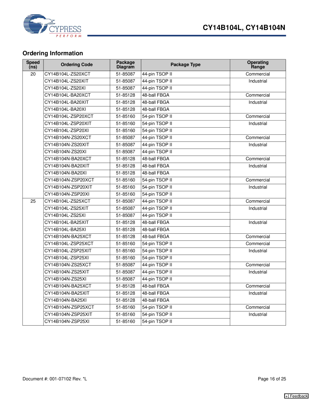
Ordering Information |
|
|
|
| |||
|
|
|
|
|
|
|
|
Speed | Ordering Code | Package | Package Type |
| Operating | ||
(ns) | Diagram |
| Range | ||||
|
|
|
|
| |||
20 |
| Commercial | |||||
|
|
|
|
|
| ||
|
| Industrial | |||||
|
|
|
|
|
| ||
|
|
| |||||
|
|
|
|
|
| ||
|
| Commercial | |||||
|
|
|
|
|
| ||
|
| Industrial | |||||
|
|
|
|
|
| ||
|
|
| |||||
|
|
|
|
|
| ||
|
| Commercial | |||||
|
|
|
|
|
| ||
|
| Industrial | |||||
|
|
|
|
|
| ||
|
|
| |||||
|
|
|
|
|
| ||
|
| Commercial | |||||
|
|
|
|
|
| ||
|
| Industrial | |||||
|
|
|
|
|
| ||
|
|
| |||||
|
|
|
|
|
| ||
|
| Commercial | |||||
|
|
|
|
|
| ||
|
| Industrial | |||||
|
|
|
|
|
| ||
|
|
| |||||
|
|
|
|
|
| ||
|
| Commercial | |||||
|
|
|
|
|
| ||
|
| Industrial | |||||
|
|
|
|
|
| ||
|
|
| |||||
|
|
|
|
|
| ||
25 |
| Commercial | |||||
|
|
|
|
|
| ||
|
| Industrial | |||||
|
|
|
|
|
| ||
|
|
| |||||
|
|
|
|
|
| ||
|
| Industrial | |||||
|
|
|
|
|
| ||
|
|
| |||||
|
|
|
|
|
| ||
|
| Commercial | |||||
|
|
|
|
|
| ||
|
| Commercial | |||||
|
|
|
|
|
| ||
|
| Industrial | |||||
|
|
|
|
|
| ||
|
|
| |||||
|
|
|
|
|
| ||
|
| Commercial | |||||
|
|
|
|
|
| ||
|
| Industrial | |||||
|
|
|
|
|
| ||
|
|
| |||||
|
|
|
|
|
| ||
|
| Commercial | |||||
|
|
|
|
|
| ||
|
| Industrial | |||||
|
|
|
|
|
| ||
|
|
| |||||
|
|
|
|
|
| ||
|
| Commercial | |||||
|
|
|
|
|
| ||
|
| Industrial | |||||
|
|
|
|
|
| ||
|
|
| |||||
|
|
|
|
|
|
|
|
Document #: | Page 16 of 25 |
[+] Feedback