Manuals
/
Cypress
/
Computer Equipment
/
Computer Hardware
Cypress
CY14B104N, CY14B104L
manual
51-85160
Models:
CY14B104L
CY14B104N
1
21
25
25
Download
25 pages
23.94 Kb
18
19
20
21
22
23
24
25
DC Electrical Characteristics
Logic Block Diagram1, 2
Hardware Recall Power Up
Switching Waveforms
Page 21
Image 21
CY14B104L, CY14B104N
Package Diagrams
(continued)
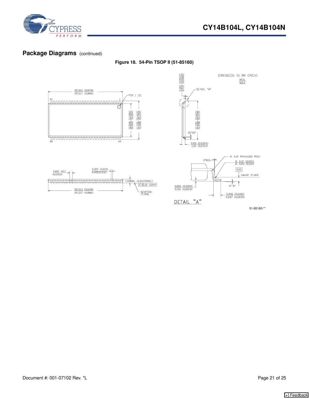
Figure 18.
54-Pin
TSOP II
(51-85160)
51-85160-**
Document #:
001-07102
Rev. *L
Page 21 of 25
[+] Feedback
Page 20
Page 22
Page 21
Image 21
Page 20
Page 22
Contents
Logic Block Diagram1, 2
Features
Functional Description
Cypress Semiconductor Corporation
Top View
Pinouts
Not to scale
Tsop
Pin Definitions
Sram Read
Device Operation
Sram Write
AutoStore Operation
Mode Selection
Hardware Recall Power Up
A15 A07 Mode Power
Software Store
Preventing AutoStore
Mode Selection A15 A07 Power
Data Protection
Noise Considerations
Maximum Ratings
DC Electrical Characteristics
Operating Range
Range
Capacitance
Data Retention and Endurance
Thermal Resistance
AC Test Conditions
Switching Waveforms
AC Switching Characteristics
Min Max
Sram Read Cycle
CY14B104L, CY14B104N
Sram Write Cycle #2 CE Controlled 3, 17, 18
AutoStore/Power Up Recall
Parameters Description CY14B104L/CY14B104N Unit Min Max
HSB
Parameters Description 20 ns 25 ns 45 ns Unit Min Max
Software Controlled STORE/RECALL Cycle
Hardware Store Cycle
Hardware Store Pulse Width
Hardware Store LOW to Store Busy 500
Inputs/Outputs2 Mode Power
Truth Table For Sram Operations
High Z
Ordering Information
CY14B104L-ZS45XIT
CY14B104L-ZS45XCT
CY14B104L-BA45XCT
CY14B104L-BA45XIT
CY 14 B 104 L ZS P 20 X C T
Part Numbering Nomenclature
ZS Tsop
Nvsram
Pin Tsop II
Package Diagrams
Ball Fbga 6 mm x 10 mm x 1.2 mm
51-85160
TUP
Document History
PCI
UHA
GVCH/PYRS
GVCH/DSG
Aesa
USB
Sales, Solutions, and Legal Information
Top
Page
Image
Contents