|
|
|
|
|
|
|
|
|
|
|
|
| CY7C1161V18, CY7C1176V18 | |||
|
|
|
|
|
|
|
|
|
|
|
|
| CY7C1163V18, CY7C1165V18 | |||
|
|
|
|
|
|
|
|
|
|
|
|
|
|
|
| |
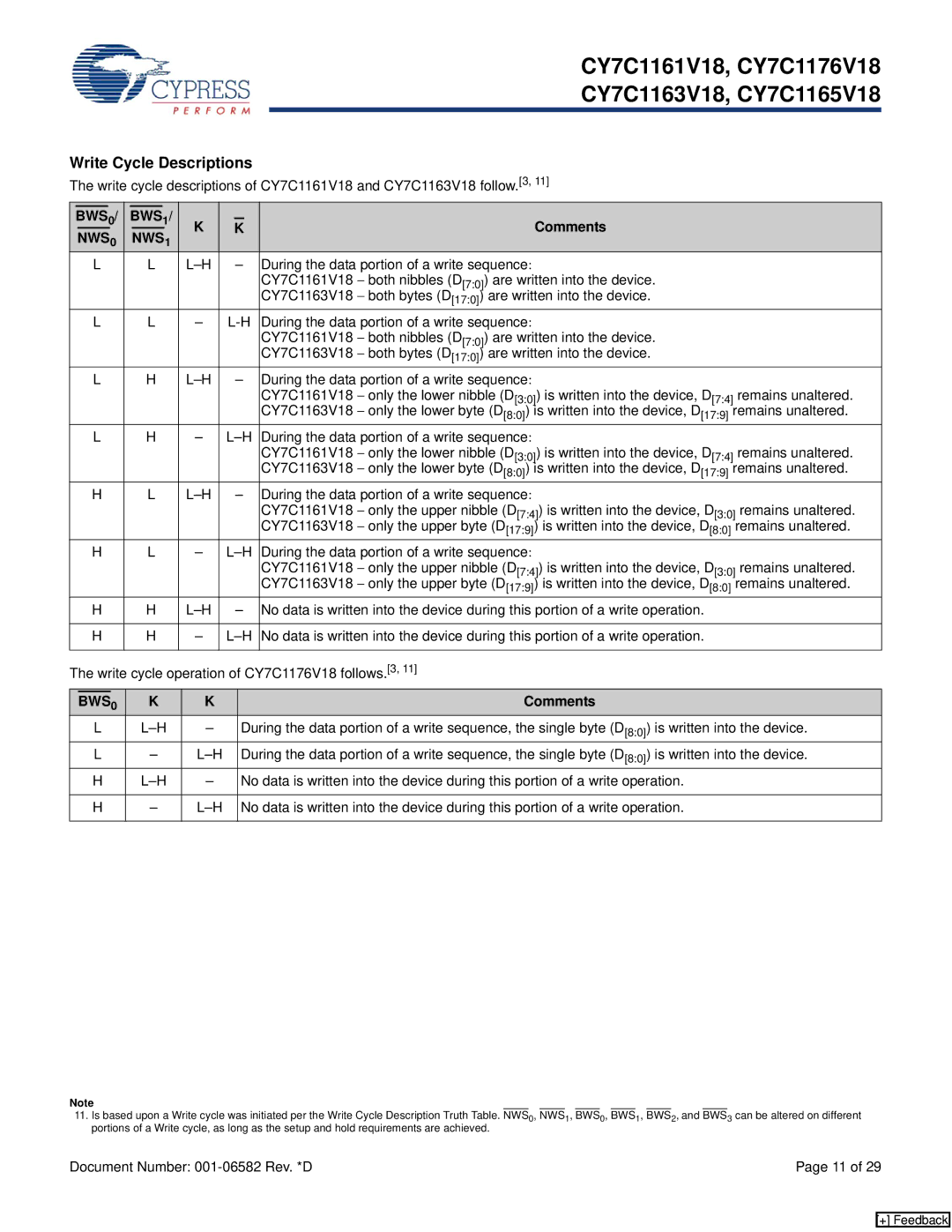
Write Cycle Descriptions |
|
|
|
|
|
| ||||||||||
The write cycle descriptions of CY7C1161V18 and CY7C1163V18 follow.[3, 11] |
|
|
| |||||||||||||
| BWS | 0/ |
| BWS | 1/ | K |
|
|
|
|
|
| Comments |
|
|
|
|
|
| K |
|
|
|
|
| ||||||||
|
|
|
|
|
|
|
|
|
|
|
|
| ||||
| NWS0 |
| NWS1 |
|
|
|
|
| ||||||||
|
|
|
|
|
|
|
|
|
|
|
|
| ||||
| L |
| L |
|
| – | During the data portion of a write sequence: |
|
|
| ||||||
|
|
|
|
|
|
|
|
|
|
| CY7C1161V18 − both nibbles (D[7:0]) are written into the device. |
|
|
| ||
|
|
|
|
|
|
|
|
|
|
| CY7C1163V18 − both bytes (D[17:0]) are written into the device. |
|
|
| ||
| L |
| L | – |
| During the data portion of a write sequence: |
|
|
| |||||||
|
|
|
|
|
|
|
|
|
|
| CY7C1161V18 − both nibbles (D[7:0]) are written into the device. |
|
|
| ||
|
|
|
|
|
|
|
|
|
|
| CY7C1163V18 − both bytes (D[17:0]) are written into the device. |
|
|
| ||
| L |
| H |
|
| – | During the data portion of a write sequence: |
|
|
| ||||||
|
|
|
|
|
|
|
|
|
|
| CY7C1161V18 − only the lower nibble (D[3:0]) is written into the device, D[7:4] | remains unaltered. | ||||
|
|
|
|
|
|
|
|
|
|
| CY7C1163V18 − only the lower byte (D[8:0]) is written into the device, D[17:9] | remains unaltered. | ||||
| L |
| H | – |
| During the data portion of a write sequence: |
|
|
| |||||||
|
|
|
|
|
|
|
|
|
|
| CY7C1161V18 − only the lower nibble (D[3:0]) is written into the device, D[7:4] | remains unaltered. | ||||
|
|
|
|
|
|
|
|
|
|
| CY7C1163V18 − only the lower byte (D[8:0]) is written into the device, D[17:9] | remains unaltered. | ||||
| H |
| L |
|
| – | During the data portion of a write sequence: |
|
|
| ||||||
|
|
|
|
|
|
|
|
|
|
| CY7C1161V18 − only the upper nibble (D[7:4]) is written into the device, D[3:0] | remains unaltered. | ||||
|
|
|
|
|
|
|
|
|
|
| CY7C1163V18 − only the upper byte (D[17:9]) is written into the device, D[8:0] | remains unaltered. | ||||
| H |
| L | – |
| During the data portion of a write sequence: |
|
|
| |||||||
|
|
|
|
|
|
|
|
|
|
| CY7C1161V18 − only the upper nibble (D[7:4]) is written into the device, D[3:0] | remains unaltered. | ||||
|
|
|
|
|
|
|
|
|
|
| CY7C1163V18 − only the upper byte (D[17:9]) is written into the device, D[8:0] | remains unaltered. | ||||
| H |
| H |
|
| – | No data is written into the device during this portion of a write operation. |
|
|
| ||||||
|
|
|
|
|
|
|
|
|
|
|
| |||||
| H |
| H | – |
| No data is written into the device during this portion of a write operation. |
|
|
| |||||||
|
|
|
|
|
|
|
|
| ||||||||
The write cycle operation of CY7C1176V18 follows.[3, 11] |
|
|
| |||||||||||||
| BWS | 0 |
| K | K |
|
|
|
|
| Comments |
|
|
| ||
| L |
| – |
| During the data portion of a write sequence, the single byte (D[8:0]) is written into the device. | |||||||||||
| L |
| – |
| During the data portion of a write sequence, the single byte (D[8:0]) is written into the device. | |||||||||||
| H |
| – |
| No data is written into the device during this portion of a write operation. |
|
|
| ||||||||
|
|
|
|
|
|
|
|
|
| |||||||
| H |
| – |
| No data is written into the device during this portion of a write operation. |
|
|
| ||||||||
|
|
|
|
|
|
|
|
|
|
|
|
|
|
|
|
|
Note
11.Is based upon a Write cycle was portions of a Write cycle, as long
initiated per the Write Cycle Description Truth Table. NWS0, NWS1, BWS0, BWS1, BWS2, and BWS3 can be altered on different as the setup and hold requirements are achieved.
Document Number: | Page 11 of 29 |
[+] Feedback