Contents
Main
CY7C1161V18, CY7C1176V18 CY7C1163V18, CY7C1165V18
18-Mbit QDR-II+ SRAM 4-Word Burst Architecture (2.5 Cycle Read Latency)
Features
Configurations
Functional Description
Selection Guide
Logic Block Diagram (CY7C1161V18)
Logic Block Diagram (CY7C1176V18)
CY7C1163V18, CY7C1165V18
Logic Block Diagram (CY7C1163V18)
Logic Block Diagram (CY7C1165V18)
Pin Configurations
CY7C1161V18 (2M x 8)
165-Ball FBGA (13 x 15 x 1.4 mm) Pinout
CY7C1176V18 (2M x 9)
CY7C1163V18, CY7C1165V18
Pin Configurations
CY7C1163V18 (1M x 18)
165-Ball FBGA (13 x 15 x 1.4 mm) Pinout
CY7C1165V18 (512K x 36)
CY7C1161V18, CY7C1176V18 CY7C1163V18, CY7C1165V18
Pin Definitions
CY7C1161V18, CY7C1176V18 CY7C1163V18, CY7C1165V18
NC NC
Pin Definitions
CY7C1161V18, CY7C1176V18 CY7C1163V18, CY7C1165V18
Functional Overview
Read Operations
Write Operations
Byte Write Operations
Depth Expansion
Programmable Impedance
Echo Clocks
Valid Data Indicator (QVLD)
DLL
Application Example
Truth Table
SRAM #1
SRAM #4
BUS MASTER (CPU or ASIC)
CY7C1161V18, CY7C1176V18 CY7C1163V18, CY7C1165V18
Write Cycle Descriptions
Page
IEEE 1149.1 Serial Boundary Scan (JTAG)
Disabling the JTAG Feature
Test Access PortTest Clock
Test Mode Select
Test Data In (TDI)
Page
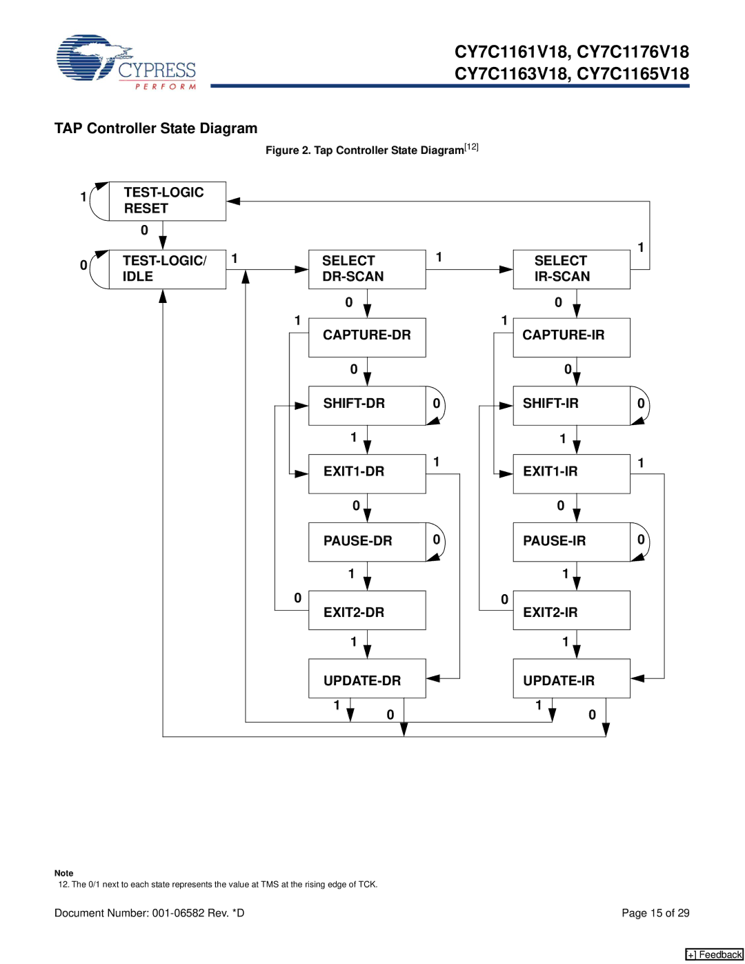
TAP Controller State Diagram
CY7C1161V18, CY7C1176V18 CY7C1163V18, CY7C1165V18
TAP Controller Block Diagram
TAP Electrical Characteristics
CY7C1161V18, CY7C1176V18
TAP AC Switching Characteristics
TAP Timing and Test Conditions
CY7C1161V18, CY7C1176V18 CY7C1163V18, CY7C1165V18
Identification Register Definitions
Scan Register Sizes
Instruction Codes
Boundary Scan Order
Power Up Sequence in QDR-II+ SRA
Power Up Sequence
DLL Constraints
Power Up Waveforms
K K
Maximum Ratings
Operating Range
Electrical Characteristics
AC Electrical Characteristics
Capacitance
Thermal Resistance
AC Test Loads and Waveforms
Page
Switching Characteristics
Switching Waveforms Read/Write/Deselect Sequence
Figure 6. Waveform for 2.5 Cycle Read Latency
[+] Feedback [+] Feedback
QVLD
t
Page
Ordering Information
Package Diagram
Figure 7. 165-Ball FBGA (13 x 15 x 1.4 mm), 51-85180
[+] Feedback [+] Feedback
SOLDER PAD TYPE : NON-SOLDER MASK DEFINED (NSMD)
1.40 MAX.
Document History Page