Manuals
/
Cypress
/
Computer Equipment
/
Computer Hardware
Cypress
CY7C1347G
manual
Electrical Characteristics continued, Capacitance, Thermal Resistance
Models:
CY7C1347G
1
10
22
22
Download
22 pages
40.69 Kb
7
8
9
10
11
12
13
14
Electrical Characteristics
Block Diagram
Single Read Accesses
Weight
psoc.cypress.com/low-power
Features
Switching Characteristics
Page 10
Image 10
Page 9
Page 11
Page 10
Image 10
Page 9
Page 11
Contents
Selection Guide
Features
CY7C1347G
Functional Description1
REGISTER
Block Diagram
ADDRESS
ADSC
Pinouts
CY7C1347G
CY7C1347G
Name
CY7C1347G
Table 1. Pin Definitions
Description
Single Write Accesses Initiated by ADSC
Single Read Accesses
Single Write Accesses Initiated by ADSP
Functional Overview
2. X = “Do Not Care.” H = Logic HIGH, L = Logic LOW
Table 5. Truth Table 2, 3, 4, 5
Operating Range
Electrical Characteristics
Maximum Ratings
VDDQ
Thermal Resistance
Electrical Characteristics continued
Capacitance
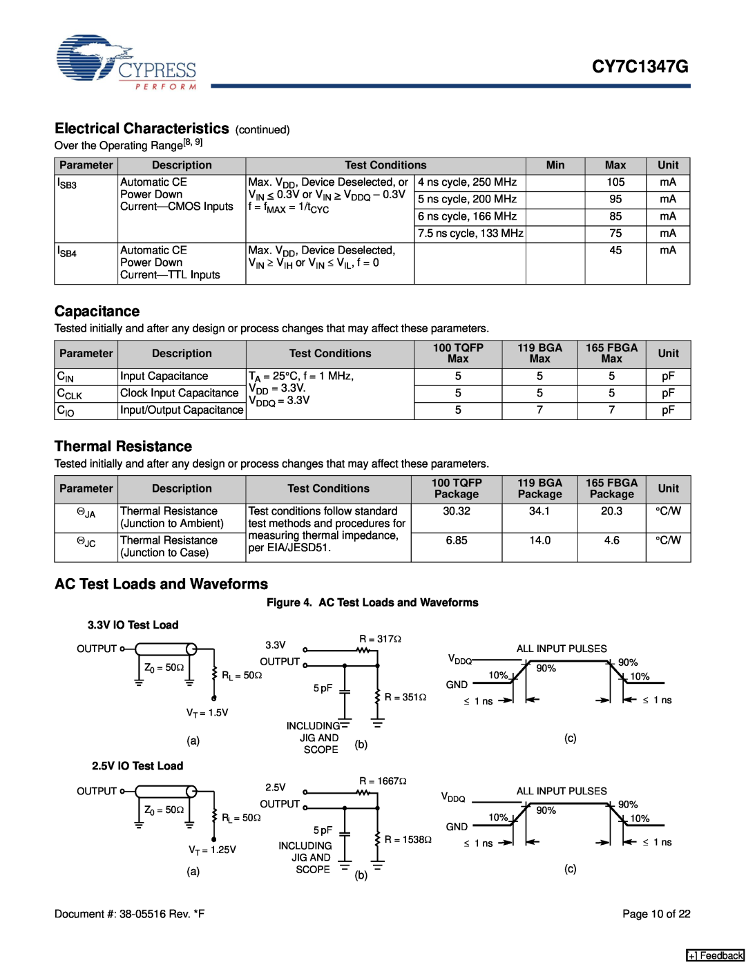
AC Test Loads and Waveforms
Switching Characteristics
Switching Waveforms
Figure 5. Read Cycle Timing16
Switching Waveforms continued
Figure 6. Write Cycle Timing16
Page 14 of
Figure 7. Read/Write Cycle Timing16, 18
19. GW is HIGH
21. DQs are in high-Z when exiting ZZ sleep mode
ALL INPUTS except ZZ
Ordering Information
Ordering Information continued
Package Diagrams
Figure 9. 100-Pin Thin Plastic Quad Flatpack 14 x 20 x 1.4 mm
Package Diagrams continued
Figure 10. 119-Ball BGA 14 x 22 x 2.4 mm
Figure 11. 165-Ball FBGA 13 x 15 x 1.4 mm
PACKAGE WEIGHT 0.475g
Page 20 of
Document Number
Document History Page
Document Title CY7C1347G 4-Mbit 128K x 36 Pipelined Sync SRAM
Submission
Worldwide Sales and Design Support
Sales, Solutions, and Legal Information
PSoC Solutions
Products
Top
Page
Image
Contents