CY7C1386D, CY7C1386F CY7C1387D, CY7C1387F
the TAP controller, it will directly control the state of the output
This bit can be set by entering the SAMPLE/PRELOAD or EXTEST command, and then shifting the desired bit into that cell, during the
register. When the EXTEST instruction is entered, this bit will directly control the output
Reserved
These instructions are not implemented but are reserved for future use. Do not use these instructions.
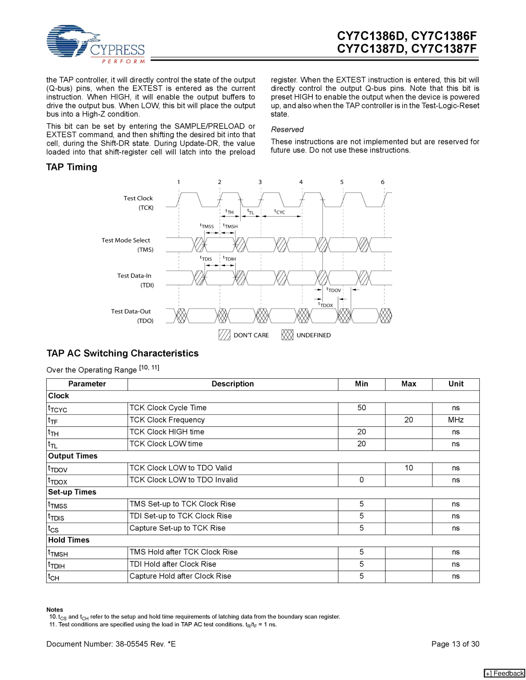
TAP Timing
1 | 2 |
Test Clock |
|
(TCK) | tTH |
| |
tTMSS | tTMSH |
Test Mode Select |
|
(TMS) |
|
tTDIS | tTDIH |
Test |
|
(TDI) |
|
Test |
|
(TDO) |
|
3
tTL tCYC
456
tTDOV
tTDOX
DON’T CARE
UNDEFINED
TAP AC Switching Characteristics
Over the Operating Range [10, 11]
Parameter | Description | Min | Max | Unit |
Clock |
|
|
|
|
|
|
|
|
|
tTCYC | TCK Clock Cycle Time | 50 |
| ns |
tTF | TCK Clock Frequency |
| 20 | MHz |
tTH | TCK Clock HIGH time | 20 |
| ns |
tTL | TCK Clock LOW time | 20 |
| ns |
Output Times |
|
|
|
|
tTDOV | TCK Clock LOW to TDO Valid |
| 10 | ns |
tTDOX | TCK Clock LOW to TDO Invalid | 0 |
| ns |
|
|
|
|
|
tTMSS | TMS | 5 |
| ns |
tTDIS | TDI | 5 |
| ns |
tCS | Capture | 5 |
| ns |
Hold Times |
|
|
|
|
|
|
|
|
|
tTMSH | TMS Hold after TCK Clock Rise | 5 |
| ns |
tTDIH | TDI Hold after Clock Rise | 5 |
| ns |
tCH | Capture Hold after Clock Rise | 5 |
| ns |
Notes
10.tCS and tCH refer to the setup and hold time requirements of latching data from the boundary scan register.
11.Test conditions are specified using the load in TAP AC test conditions. tR/tF = 1 ns.
Document Number: | Page 13 of 30 |
[+] Feedback