CY7C1386D, CY7C1386F
CY7C1387D, CY7C1387F
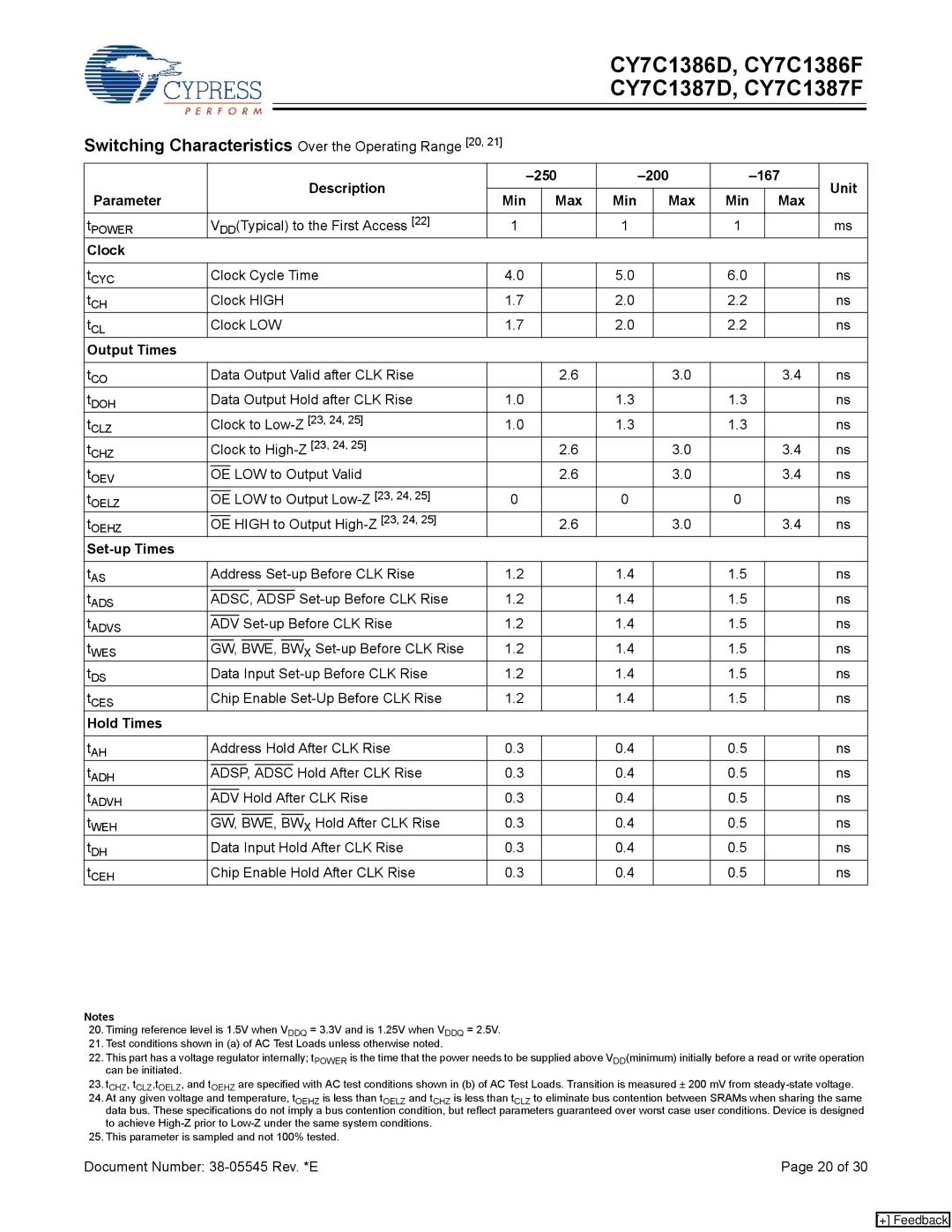
Switching Characteristics Over the Operating Range [20, 21]
|
|
|
|
|
|
|
|
|
|
|
|
|
|
| Description |
|
|
|
| Unit | |||
|
|
|
|
|
|
|
|
|
|
|
|
|
|
|
|
|
|
|
|
|
| ||
Parameter |
|
|
|
|
|
|
|
|
|
|
|
|
|
| Min | Max | Min |
| Max | Min | Max | ||
|
|
|
|
|
|
|
|
|
|
|
|
|
|
|
|
| |||||||
|
|
|
|
|
|
|
|
|
|
| |||||||||||||
tPOWER |
| VDD(Typical) to the First Access [22] | 1 |
| 1 |
|
| 1 |
| ms | |||||||||||||
Clock |
|
|
|
|
|
|
|
|
|
|
|
|
|
|
|
|
|
|
|
|
|
| |
|
|
|
|
|
|
|
|
|
| ||||||||||||||
tCYC |
| Clock Cycle Time | 4.0 |
| 5.0 |
|
| 6.0 |
| ns | |||||||||||||
tCH |
| Clock HIGH | 1.7 |
| 2.0 |
|
| 2.2 |
| ns | |||||||||||||
tCL |
| Clock LOW | 1.7 |
| 2.0 |
|
| 2.2 |
| ns | |||||||||||||
Output Times |
|
|
|
|
|
|
|
|
|
|
|
|
|
|
|
|
|
|
|
|
|
| |
|
|
|
|
|
|
|
|
|
| ||||||||||||||
tCO |
| Data Output Valid after CLK Rise |
| 2.6 |
|
| 3.0 |
| 3.4 | ns | |||||||||||||
tDOH |
| Data Output Hold after CLK Rise | 1.0 |
| 1.3 |
|
| 1.3 |
| ns | |||||||||||||
tCLZ |
| Clock to | 1.0 |
| 1.3 |
|
| 1.3 |
| ns | |||||||||||||
tCHZ |
| Clock to |
| 2.6 |
|
| 3.0 |
| 3.4 | ns | |||||||||||||
tOEV |
|
|
| LOW to Output Valid |
| 2.6 |
|
| 3.0 |
| 3.4 | ns | |||||||||||
OE |
|
|
| ||||||||||||||||||||
tOELZ |
|
|
| LOW to Output | 0 |
| 0 |
|
| 0 |
| ns | |||||||||||
OE |
|
|
|
| |||||||||||||||||||
tOEHZ |
|
|
| HIGH to Output |
| 2.6 |
|
| 3.0 |
| 3.4 | ns | |||||||||||
OE |
|
|
| ||||||||||||||||||||
|
|
|
|
|
|
|
|
|
|
|
|
|
|
|
|
|
|
|
|
|
|
| |
|
|
|
|
|
|
|
|
|
| ||||||||||||||
tAS |
| Address | 1.2 |
| 1.4 |
|
| 1.5 |
| ns | |||||||||||||
tADS |
|
|
|
|
|
|
|
|
|
|
|
|
| 1.2 |
| 1.4 |
|
| 1.5 |
| ns | ||
ADSC, | ADSP |
|
|
|
| ||||||||||||||||||
tADVS |
|
|
|
|
| 1.2 |
| 1.4 |
|
| 1.5 |
| ns | ||||||||||
ADV |
|
|
|
| |||||||||||||||||||
tWES |
|
|
|
|
|
|
|
|
|
|
|
|
| X | 1.2 |
| 1.4 |
|
| 1.5 |
| ns | |
GW, | BWE, | BW |
|
|
|
| |||||||||||||||||
tDS |
| Data Input | 1.2 |
| 1.4 |
|
| 1.5 |
| ns | |||||||||||||
tCES |
| Chip Enable | 1.2 |
| 1.4 |
|
| 1.5 |
| ns | |||||||||||||
Hold Times |
|
|
|
|
|
|
|
|
|
|
|
|
|
|
|
|
|
|
|
|
|
| |
|
|
|
|
|
|
|
|
|
| ||||||||||||||
tAH |
| Address Hold After CLK Rise | 0.3 |
| 0.4 |
|
| 0.5 |
| ns | |||||||||||||
tADH |
|
|
|
|
|
|
|
|
|
|
| Hold After CLK Rise | 0.3 |
| 0.4 |
|
| 0.5 |
| ns | |||
ADSP, | ADSC |
|
|
|
| ||||||||||||||||||
tADVH |
|
|
|
| Hold After CLK Rise | 0.3 |
| 0.4 |
|
| 0.5 |
| ns | ||||||||||
ADV |
|
|
|
| |||||||||||||||||||
tWEH |
|
|
|
|
|
|
|
|
|
|
|
|
| X Hold After CLK Rise | 0.3 |
| 0.4 |
|
| 0.5 |
| ns | |
GW, | BWE, | BW |
|
|
|
| |||||||||||||||||
tDH |
| Data Input Hold After CLK Rise | 0.3 |
| 0.4 |
|
| 0.5 |
| ns | |||||||||||||
tCEH |
| Chip Enable Hold After CLK Rise | 0.3 |
| 0.4 |
|
| 0.5 |
| ns | |||||||||||||
Notes
20.Timing reference level is 1.5V when VDDQ = 3.3V and is 1.25V when VDDQ = 2.5V.
21.Test conditions shown in (a) of AC Test Loads unless otherwise noted.
22.This part has a voltage regulator internally; tPOWER is the time that the power needs to be supplied above VDD(minimum) initially before a read or write operation can be initiated.
23.tCHZ, tCLZ,tOELZ, and tOEHZ are specified with AC test conditions shown in (b) of AC Test Loads. Transition is measured ± 200 mV from
24.At any given voltage and temperature, tOEHZ is less than tOELZ and tCHZ is less than tCLZ to eliminate bus contention between SRAMs when sharing the same data bus. These specifications do not imply a bus contention condition, but reflect parameters guaranteed over worst case user conditions. Device is designed to achieve
25.This parameter is sampled and not 100% tested.
Document Number: | Page 20 of 30 |
[+] Feedback