CY7C1386D, CY7C1386F
CY7C1387D, CY7C1387F
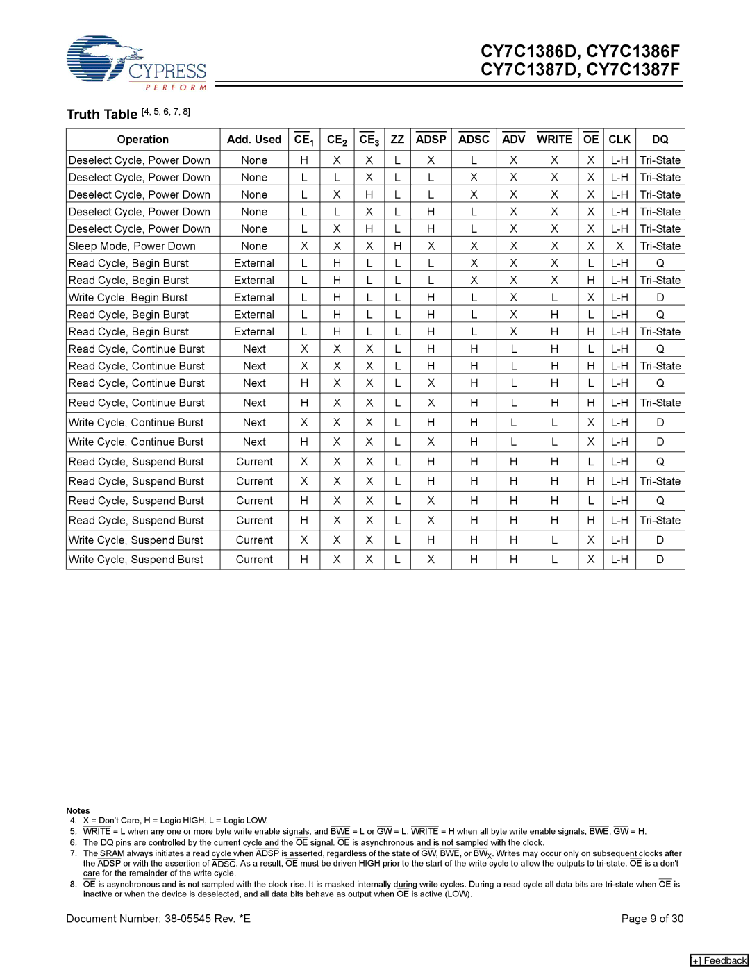
Truth Table [4, 5, 6, 7, 8]
|
|
|
|
|
|
|
|
|
|
|
|
|
|
|
|
|
|
|
|
|
|
|
|
|
|
|
Operation | Add. Used |
| CE1 | CE2 |
| CE3 | ZZ | ADSP |
|
| ADSC |
| ADV |
|
| WRITE |
| OE |
| CLK | DQ | |||||
Deselect Cycle, Power Down | None |
| H | X |
| X | L |
| X |
|
| L |
| X |
|
| X |
| X |
| ||||||
Deselect Cycle, Power Down | None |
| L | L |
| X | L |
| L |
|
| X |
| X |
|
| X |
| X |
| ||||||
Deselect Cycle, Power Down | None |
| L | X |
| H | L |
| L |
|
| X |
| X |
|
| X |
| X |
| ||||||
Deselect Cycle, Power Down | None |
| L | L |
| X | L |
| H |
|
| L |
| X |
|
| X |
| X |
| ||||||
Deselect Cycle, Power Down | None |
| L | X |
| H | L |
| H |
|
| L |
| X |
|
| X |
| X |
| ||||||
Sleep Mode, Power Down | None |
| X | X |
| X | H |
| X |
|
| X |
| X |
|
| X |
| X |
| X | |||||
Read Cycle, Begin Burst | External |
| L | H |
| L | L |
| L |
|
| X |
| X |
|
| X |
| L |
| Q | |||||
Read Cycle, Begin Burst | External |
| L | H |
| L | L |
| L |
|
| X |
| X |
|
| X |
| H |
| ||||||
Write Cycle, Begin Burst | External |
| L | H |
| L | L |
| H |
|
| L |
| X |
|
| L |
| X |
| D | |||||
Read Cycle, Begin Burst | External |
| L | H |
| L | L |
| H |
|
| L |
| X |
|
| H |
| L |
| Q | |||||
Read Cycle, Begin Burst | External |
| L | H |
| L | L |
| H |
|
| L |
| X |
|
| H |
| H |
| ||||||
Read Cycle, Continue Burst | Next |
| X | X |
| X | L |
| H |
|
| H |
| L |
|
| H |
| L |
| Q | |||||
Read Cycle, Continue Burst | Next |
| X | X |
| X | L |
| H |
|
| H |
| L |
|
| H |
| H |
| ||||||
Read Cycle, Continue Burst | Next |
| H | X |
| X | L |
| X |
|
| H |
| L |
|
| H |
| L |
| Q | |||||
|
|
|
|
|
|
|
|
|
|
|
|
|
|
|
|
|
|
|
|
|
|
| ||||
Read Cycle, Continue Burst | Next |
| H | X |
| X | L |
| X |
|
| H |
| L |
|
| H |
| H |
| ||||||
|
|
|
|
|
|
|
|
|
|
|
|
|
|
|
|
|
|
|
|
|
|
| ||||
Write Cycle, Continue Burst | Next |
| X | X |
| X | L |
| H |
|
| H |
| L |
|
| L |
| X |
| D | |||||
|
|
|
|
|
|
|
|
|
|
|
|
|
|
|
|
|
|
|
|
|
|
| ||||
Write Cycle, Continue Burst | Next |
| H | X |
| X | L |
| X |
|
| H |
| L |
|
| L |
| X |
| D | |||||
|
|
|
|
|
|
|
|
|
|
|
|
|
|
|
|
|
|
|
|
|
|
| ||||
Read Cycle, Suspend Burst | Current |
| X | X |
| X | L |
| H |
|
| H |
| H |
|
| H |
| L |
| Q | |||||
|
|
|
|
|
|
|
|
|
|
|
|
|
|
|
|
|
|
|
|
|
|
| ||||
Read Cycle, Suspend Burst | Current |
| X | X |
| X | L |
| H |
|
| H |
| H |
|
| H |
| H |
| ||||||
|
|
|
|
|
|
|
|
|
|
|
|
|
|
|
|
|
|
|
|
|
|
| ||||
Read Cycle, Suspend Burst | Current |
| H | X |
| X | L |
| X |
|
| H |
| H |
|
| H |
| L |
| Q | |||||
|
|
|
|
|
|
|
|
|
|
|
|
|
|
|
|
|
|
|
|
|
|
| ||||
Read Cycle, Suspend Burst | Current |
| H | X |
| X | L |
| X |
|
| H |
| H |
|
| H |
| H |
| ||||||
|
|
|
|
|
|
|
|
|
|
|
|
|
|
|
|
|
|
|
|
|
|
| ||||
Write Cycle, Suspend Burst | Current |
| X | X |
| X | L |
| H |
|
| H |
| H |
|
| L |
| X |
| D | |||||
|
|
|
|
|
|
|
|
|
|
|
|
|
|
|
|
|
|
|
|
|
|
| ||||
Write Cycle, Suspend Burst | Current |
| H | X |
| X | L |
| X |
|
| H |
| H |
|
| L |
| X |
| D | |||||
|
|
|
|
|
|
|
|
|
|
|
|
|
|
|
|
|
|
|
|
|
|
|
|
|
|
|
Notes
4.X = Don't Care, H = Logic HIGH, L = Logic LOW.
5.WRITE = L when any one or more byte write enable signals, and BWE = L or GW = L. WRITE = H when all byte write enable signals, BWE, GW = H.
6.The DQ pins are controlled by the current cycle and the OE signal. OE is asynchronous and is not sampled with the clock.
7.The SRAM always initiates a read cycle when ADSP is asserted, regardless of the state of GW, BWE, or BWX. Writes may occur only on subsequent clocks after the ADSP or with the assertion of ADSC. As a result, OE must be driven HIGH prior to the start of the write cycle to allow the outputs to
8.OE is asynchronous and is not sampled with the clock rise. It is masked internally during write cycles. During a read cycle all data bits are
Document Number: | Page 9 of 30 |
[+] Feedback