CY7C1470BV25
CY7C1472BV25, CY7C1474BV25
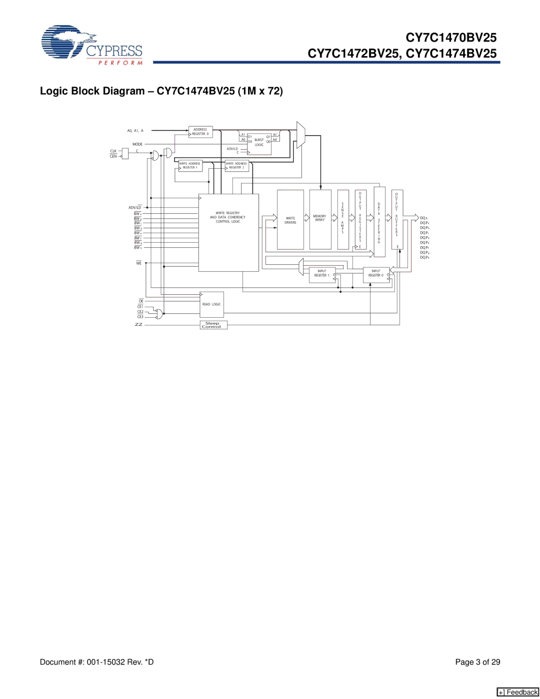
Logic Block Diagram – CY7C1474BV25 (1M x 72)
| A0, A1, A | ADDRESS |
|
|
|
|
|
|
|
|
|
| |
|
| REGISTER 0 | A1 | D1 |
| Q1 | A1' |
|
|
|
|
| |
|
|
|
|
|
|
|
|
|
| ||||
| MODE |
|
| A0 | D0 | BURST | Q0 | A0' |
|
|
|
|
|
|
|
| ADV/LD |
| LOGIC |
|
|
|
|
|
|
| |
CLK | C |
|
|
|
|
|
|
|
|
|
|
| |
|
| C |
|
|
|
|
|
|
|
|
| ||
CEN |
|
|
|
|
|
|
|
|
|
|
|
| |
|
|
|
|
|
|
|
|
|
|
|
|
| |
|
| WRITE ADDRESS |
| WRITE ADDRESS |
|
|
|
|
|
|
|
|
|
|
| REGISTER 1 |
| REGISTER 2 |
|
|
|
|
|
|
|
|
|
|
|
|
|
|
|
|
|
|
|
| O |
| O |
|
|
|
|
|
|
|
|
|
|
| U |
| U |
|
|
|
|
|
|
|
|
|
|
| T |
| T |
| ADV/LD |
|
|
|
|
|
|
|
| S | P | D | P |
|
|
|
|
|
|
|
|
| E | U | A | U | |
| BW a |
|
| WRITE REGISTRY |
|
|
|
|
| N | T | T | T |
|
|
|
|
|
|
| MEMORY | S | R | A |
| ||
| BW b |
|
| AND DATA COHERENCY |
|
|
| WRITE | E | S | B | ||
|
|
| CONTROL LOGIC |
|
|
| ARRAY | A | E | U | |||
| BW c |
|
|
|
|
| DRIVERS |
| G | T | F | ||
| BW d |
|
|
|
|
|
|
|
| M | I | E | F |
|
|
|
|
|
|
|
|
| P | S | E | E | |
| BW e |
|
|
|
|
|
|
|
| S | T | R | R |
|
|
|
|
|
|
|
|
| E | ||||
| BW f |
|
|
|
|
|
|
|
|
| I | S | |
|
|
|
|
|
|
|
|
|
| R | N |
| |
| BW g |
|
|
|
|
|
|
|
|
| S | G |
|
|
|
|
|
|
|
|
|
|
| E | E | ||
| BW h |
|
|
|
|
|
|
|
|
|
| ||
| WE |
|
|
|
|
|
|
|
|
|
|
|
|
|
|
|
|
|
|
|
|
| INPUT | E |
| INPUT | E |
|
|
|
|
|
|
|
|
| REGISTER 1 |
| REGISTER 0 | ||
| OE |
| READ LOGIC |
|
|
|
|
|
|
|
|
| |
| CE1 |
|
|
|
|
|
|
|
|
|
| ||
|
|
|
|
|
|
|
|
|
|
|
|
| |
| CE2 |
|
|
|
|
|
|
|
|
|
|
|
|
| CE3 |
|
|
|
|
|
|
|
|
|
|
|
|
| ZZ |
| Sleep |
|
|
|
|
|
|
|
|
| |
|
|
| Control |
|
|
|
|
|
|
|
|
| |
DQ s DQ Pa DQ Pb DQ Pc DQ Pd DQ Pe DQ Pf DQ Pg DQ Ph
Document #: | Page 3 of 29 |
[+] Feedback