CY7C64215
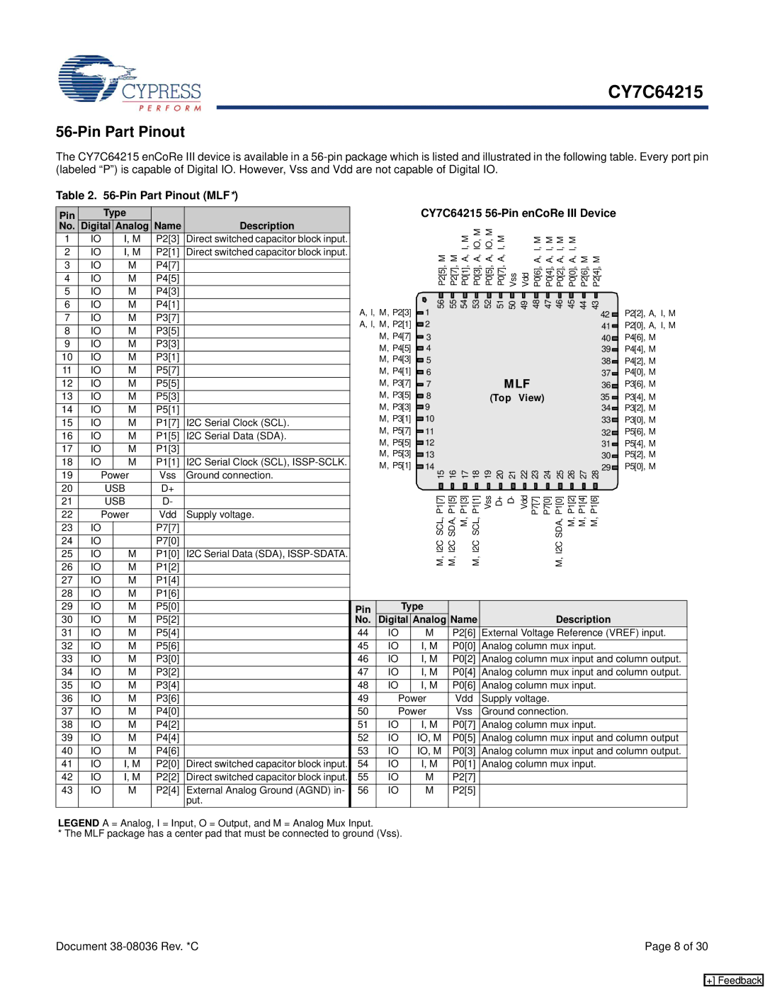
56-Pin Part Pinout
The CY7C64215 enCoRe III device is available in a
Table 2. |
|
|
|
|
|
|
|
|
|
|
|
|
|
|
|
|
|
|
|
|
|
|
|
|
|
|
|
|
|
|
|
|
|
| |||||
|
|
|
|
|
|
|
|
|
| CY7C64215 |
| ||||||||||||||||||||||||||||
Pin |
| Type |
|
|
|
|
|
| |||||||||||||||||||||||||||||||
No. | Digital | Analog | Name | Description |
|
|
|
|
|
|
|
|
|
| I, M IO, M | IO, M I, M |
|
|
|
|
|
|
|
|
|
|
|
|
|
|
| ||||||||
1 | IO |
| I, M | P2[3] | Direct switched capacitor block input. |
|
|
|
|
|
|
|
|
|
|
|
| I, M I, M I, M I, M |
|
|
|
|
|
| |||||||||||||||
2 | IO |
| I, M | P2[1] | Direct switched capacitor block input. |
|
|
|
|
|
|
|
|
|
|
|
|
|
|
|
|
|
| ||||||||||||||||
|
|
|
|
|
|
| M M A, A, A, A, |
|
| A, A, A, A, M M |
| ||||||||||||||||||||||||||||
3 | IO |
| M | P4[7] |
|
|
|
|
|
|
|
|
|
| |||||||||||||||||||||||||
|
|
|
|
|
|
|
| P2[5], | P2[7], | P0[1], | P0[3], | P0[5], P0[7], Vss Vdd | P0[6], P0[4], | P0[2], | P0[0], | P2[6], | P2[4], |
| |||||||||||||||||||||
4 | IO |
| M | P4[5] |
|
|
|
|
|
|
|
|
|
|
|
|
|
|
|
|
|
|
|
|
|
|
|
|
|
|
|
|
|
|
|
|
|
|
|
5 | IO |
| M | P4[3] |
|
|
|
|
|
|
|
|
|
|
|
|
|
|
|
|
|
|
|
|
|
|
|
|
|
|
|
|
|
|
|
|
|
|
|
|
|
|
|
|
|
|
|
|
|
|
|
|
|
|
|
|
|
|
|
|
|
|
|
|
|
|
|
|
|
|
|
|
|
|
| ||||
6 | IO |
| M | P4[1] |
| A, I, M, P2[3] |
|
| 1 | 56 55 54 53 52 51 50 49 | 48 47 46 45 44 43 |
| P2[2], A, I, M | ||||||||||||||||||||||||||
|
|
|
|
|
|
|
|
|
|
|
|
|
|
|
|
|
|
|
|
|
|
|
|
|
|
|
|
|
|
|
| 42 |
| ||||||
7 | IO |
| M | P3[7] |
| A, I, M, P2[1] |
|
| 2 |
|
|
|
|
|
|
|
|
|
|
|
|
|
|
|
|
|
|
|
|
|
|
|
| 41 |
| P2[0], A, I, M | |||
|
|
|
|
|
|
|
|
|
|
|
|
|
|
|
|
|
|
|
|
|
|
|
|
|
|
|
|
|
|
|
|
| |||||||
8 | IO |
| M | P3[5] |
|
| M, P4[7] |
|
| 3 |
|
|
|
|
|
|
|
|
|
|
|
|
|
|
|
|
|
|
|
|
|
|
|
| 40 |
| P4[6], M | ||
|
|
|
|
|
|
|
|
|
|
|
|
|
|
|
|
|
|
|
|
|
|
|
|
|
|
|
|
|
|
|
|
|
| ||||||
9 | IO |
| M | P3[3] |
|
|
|
|
|
|
|
|
|
|
|
|
|
|
|
|
|
|
|
|
|
|
|
|
|
|
| ||||||||
|
|
| M, P4[5] |
|
| 4 |
|
|
|
|
|
|
|
|
|
|
|
|
|
|
|
|
|
|
|
|
|
|
|
| 39 |
| P4[4], M | ||||||
|
|
|
|
|
|
|
|
|
|
|
|
|
|
|
|
|
|
|
|
|
|
|
|
|
|
|
|
|
|
|
|
|
| ||||||
10 | IO |
| M | P3[1] |
|
| M, P4[3] |
|
| 5 |
|
|
|
|
|
|
|
|
|
|
|
|
|
|
|
|
|
|
|
|
|
|
|
| 38 |
| P4[2], M | ||
|
|
|
|
|
|
|
|
|
|
|
|
|
|
|
|
|
|
|
|
|
|
|
|
|
|
|
|
|
| ||||||||||
11 | IO |
| M | P5[7] |
|
| M, P4[1] |
|
| 6 |
|
|
|
|
|
|
|
|
|
| MLF |
|
|
|
|
|
|
|
|
| 37 |
| P4[0], M | ||||||
|
|
|
|
|
|
|
|
|
|
|
|
|
|
|
|
|
|
|
|
|
|
|
|
| |||||||||||||||
12 | IO |
| M | P5[5] |
|
| M, P3[7] |
|
| 7 |
|
|
|
|
|
|
|
|
|
|
|
|
|
|
|
|
|
|
| 36 |
| P3[6], M | |||||||
|
|
|
|
|
|
|
|
|
|
|
|
|
|
|
|
|
|
|
|
|
|
|
|
| |||||||||||||||
13 | IO |
| M | P5[3] |
|
| M, P3[5] |
|
| 8 |
|
|
|
|
|
|
|
|
| (Top | View) |
|
|
|
|
|
| 35 |
| P3[4], M | |||||||||
|
|
|
|
|
|
|
|
|
|
|
|
|
|
|
|
|
|
|
|
| |||||||||||||||||||
|
|
|
|
|
|
| M, P3[3] |
| 9 |
|
|
|
|
|
|
|
|
|
|
|
|
|
|
|
|
|
|
|
|
|
|
|
| 34 |
| P3[2], M | |||
14 | IO |
| M | P5[1] |
|
|
|
|
|
|
|
|
|
|
|
|
|
|
|
|
|
|
|
|
|
|
|
|
|
| |||||||||
|
|
|
|
|
|
|
|
|
|
|
|
|
|
|
|
|
|
|
|
|
|
|
|
|
|
|
|
|
| ||||||||||
|
|
|
|
|
|
| M, P3[1] |
| 10 |
|
|
|
|
|
|
|
|
|
|
|
|
|
|
|
|
|
|
|
|
|
|
|
| 33 |
| P3[0], M | |||
15 | IO |
| M | P1[7] | I2C Serial Clock (SCL). |
|
|
|
|
|
|
|
|
|
|
|
|
|
|
|
|
|
|
|
|
|
|
|
|
| |||||||||
|
|
|
|
|
|
|
|
|
|
|
|
|
|
|
|
|
|
|
|
|
|
|
|
|
|
|
|
| |||||||||||
|
|
|
|
|
|
| M, P5[7] |
| 11 |
|
|
|
|
|
|
|
|
|
|
|
|
|
|
|
|
|
|
|
|
|
|
|
| 32 |
| P5[6], M | |||
16 | IO |
| M | P1[5] | I2C Serial Data (SDA). |
|
|
|
|
|
|
|
|
|
|
|
|
|
|
|
|
|
|
|
|
|
|
|
|
| |||||||||
|
| M, P5[5] |
|
| 12 |
|
|
|
|
|
|
|
|
|
|
|
|
|
|
|
|
|
|
|
|
|
|
|
| 31 |
| P5[4], M | |||||||
|
|
|
|
|
|
|
|
|
|
|
|
|
|
|
|
|
|
|
|
|
|
|
|
|
|
|
|
|
|
|
|
| |||||||
17 | IO |
| M | P1[3] |
|
| M, P5[3] |
|
| 13 |
|
|
|
|
|
|
|
|
|
|
|
|
|
|
|
|
|
|
|
|
|
|
|
| 30 |
| P5[2], M | ||
18 | IO |
| M | P1[1] | I2C Serial Clock (SCL), |
| M, P5[1] |
|
| 14 | 15 16 17 18 19 20 21 | 22 |
|
|
|
|
|
|
|
|
| 29 |
| P5[0], M | |||||||||||||||
19 | Power | Vss | Ground connection. |
|
|
|
|
|
| 23 24 | 25 26 27 28 |
|
| ||||||||||||||||||||||||||
20 |
| USB | D+ |
|
|
|
|
|
|
|
|
|
|
|
|
|
|
|
|
|
|
|
|
|
|
|
|
|
|
|
|
|
|
|
|
|
|
| |
|
|
|
|
|
|
|
| P1[7] | P1[5] | P1[3] | P1[1] | Vss D+ | Vdd | P7[7] P7[0] | P1[0] | P1[2] | P1[4] | P1[6] |
| ||||||||||||||||||||
21 |
| USB | D- |
|
|
|
|
|
|
|
|
|
|
|
|
|
|
|
|
|
|
|
|
|
|
|
|
|
|
|
|
|
|
|
|
|
|
| |
22 | Power | Vdd | Supply voltage. |
|
|
|
|
|
| SCL, | SDA, | M, | SCL, |
|
|
|
|
|
|
|
|
|
| SDA, | M, | M, | M, |
| |||||||||||
23 | IO |
|
| P7[7] |
|
|
|
|
|
|
|
|
|
|
|
|
|
|
|
|
|
|
|
|
|
|
|
|
|
|
|
|
|
|
|
|
|
|
|
24 | IO |
|
| P7[0] |
|
|
|
|
|
|
| I2C | I2C |
|
| I2C |
|
|
|
|
|
|
|
|
|
| I2C |
|
|
|
|
|
|
|
| ||||
25 | IO |
| M | P1[0] | I2C Serial Data (SDA), |
|
|
|
|
|
|
|
|
|
|
|
|
|
|
|
|
|
|
|
|
|
|
|
|
|
| ||||||||
|
|
|
|
|
|
| M, M, |
|
| M, |
|
|
|
|
|
|
|
|
|
| M, |
|
|
|
|
|
|
|
| ||||||||||
26 | IO |
| M | P1[2] |
|
|
|
|
|
|
|
|
|
|
|
|
|
|
|
|
|
|
|
|
|
|
|
|
|
|
| ||||||||
|
|
|
|
|
|
|
|
|
|
|
|
|
|
|
|
|
|
|
|
|
|
|
|
|
|
|
|
|
|
|
|
|
|
|
| ||||
27 | IO |
| M | P1[4] |
|
|
|
|
|
|
|
|
|
|
|
|
|
|
|
|
|
|
|
|
|
|
|
|
|
|
|
|
|
|
|
|
|
|
|
28 | IO |
| M | P1[6] |
|
|
|
|
|
|
|
|
|
|
|
|
|
|
|
|
|
|
|
|
|
|
|
|
|
|
|
|
|
|
|
|
|
|
|
29 | IO |
| M | P5[0] |
| Pin | Type |
|
| Name |
|
|
|
|
|
|
|
|
|
| Description |
| |||||||||||||||||
30 | IO |
| M | P5[2] |
| No. | Digital | Analog |
|
|
|
|
|
|
|
|
|
|
| ||||||||||||||||||||
31 | IO |
| M | P5[4] |
| 44 | IO |
|
|
| M |
|
|
| P2[6] | External Voltage Reference (VREF) input. | |||||||||||||||||||||||
32 | IO |
| M | P5[6] |
| 45 | IO |
|
| I, M |
| P0[0] | Analog column mux input. |
| |||||||||||||||||||||||||
33 | IO |
| M | P3[0] |
| 46 | IO |
|
| I, M |
| P0[2] | Analog column mux input and column output. | ||||||||||||||||||||||||||
34 | IO |
| M | P3[2] |
| 47 | IO |
|
| I, M |
| P0[4] | Analog column mux input and column output. | ||||||||||||||||||||||||||
35 | IO |
| M | P3[4] |
| 48 | IO |
|
| I, M |
| P0[6] | Analog column mux input. |
| |||||||||||||||||||||||||
36 | IO |
| M | P3[6] |
| 49 | Power |
|
|
| Vdd | Supply voltage. |
|
|
|
|
|
|
|
|
|
| |||||||||||||||||
37 | IO |
| M | P4[0] |
| 50 | Power |
|
|
| Vss | Ground connection. |
|
|
|
|
|
| |||||||||||||||||||||
38 | IO |
| M | P4[2] |
| 51 | IO |
|
| I, M |
| P0[7] | Analog column mux input. |
| |||||||||||||||||||||||||
39 | IO |
| M | P4[4] |
| 52 | IO |
| IO, M |
| P0[5] | Analog column mux input and column output | |||||||||||||||||||||||||||
40 | IO |
| M | P4[6] |
| 53 | IO |
| IO, M |
| P0[3] | Analog column mux input and column output. | |||||||||||||||||||||||||||
41 | IO |
| I, M | P2[0] | Direct switched capacitor block input. | 54 | IO |
|
| I, M |
| P0[1] | Analog column mux input. |
| |||||||||||||||||||||||||
42 | IO |
| I, M | P2[2] | Direct switched capacitor block input. | 55 | IO |
|
|
| M |
|
|
| P2[7] |
|
|
|
|
|
|
|
|
|
|
|
|
|
|
|
|
|
|
|
| ||||
43 | IO |
| M | P2[4] | External Analog Ground (AGND) in- | 56 | IO |
|
|
| M |
|
|
| P2[5] |
|
|
|
|
|
|
|
|
|
|
|
|
|
|
|
|
|
|
|
| ||||
|
|
|
|
| put. |
|
|
|
|
|
|
|
|
|
|
|
|
|
|
|
|
|
|
|
|
|
|
|
|
|
|
|
|
|
|
|
|
|
|
LEGEND A = Analog, I = Input, O = Output, and M = Analog Mux Input.
* The MLF package has a center pad that must be connected to ground (Vss).
Document | Page 8 of 30 |
[+] Feedback