CY7C64215
28-Pin Part Pinout
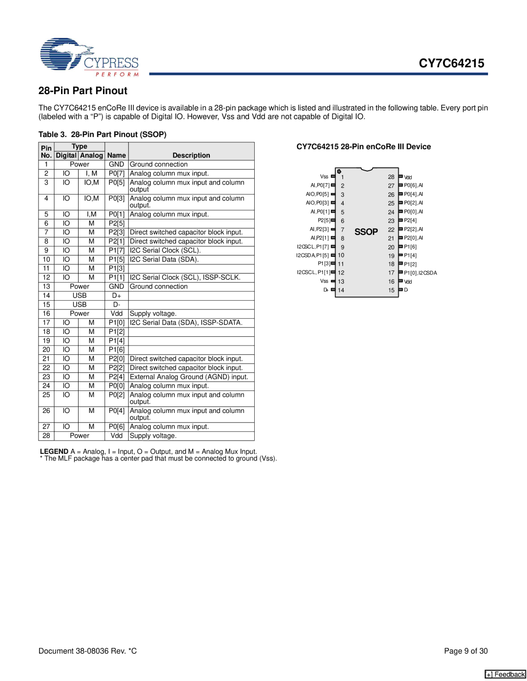
The CY7C64215 enCoRe III device is available in a
Table 3. 28-Pin Part Pinout (SSOP)
Pin | Type |
|
| |
No. | Digital | Analog | Name | Description |
1 | Power | GND | Ground connection | |
CY7C64215 28-Pin enCoRe III Device
2 | IO |
| I, M | P0[7] | Analog column mux input. |
3 | IO |
| IO,M | P0[5] | Analog column mux input and column |
|
|
|
|
| output |
4 | IO |
| IO,M | P0[3] | Analog column mux input and column |
|
|
|
|
| output. |
5 | IO |
| I,M | P0[1] | Analog column mux input. |
6 | IO |
| M | P2[5] |
|
7 | IO |
| M | P2[3] | Direct switched capacitor block input. |
8 | IO |
| M | P2[1] | Direct switched capacitor block input. |
9 | IO |
| M | P1[7] | I2C Serial Clock (SCL). |
10 | IO |
| M | P1[5] | I2C Serial Data (SDA). |
11 | IO |
| M | P1[3] |
|
12 | IO |
| M | P1[1] | I2C Serial Clock (SCL), |
13 | Power | GND | Ground connection | ||
14 |
| USB | D+ |
| |
15 |
| USB | D- |
| |
16 | Power | Vdd | Supply voltage. | ||
17 | IO |
| M | P1[0] | I2C Serial Data (SDA), |
18 | IO |
| M | P1[2] |
|
19 | IO |
| M | P1[4] |
|
20 | IO |
| M | P1[6] |
|
21 | IO |
| M | P2[0] | Direct switched capacitor block input. |
22 | IO |
| M | P2[2] | Direct switched capacitor block input. |
23 | IO |
| M | P2[4] | External Analog Ground (AGND) input. |
24 | IO |
| M | P0[0] | Analog column mux input. |
25 | IO |
| M | P0[2] | Analog column mux input and column |
|
|
|
|
| output. |
26 | IO |
| M | P0[4] | Analog column mux input and column |
|
|
|
|
| output. |
27 | IO |
| M | P0[6] | Analog column mux input. |
28 | Power | Vdd | Supply voltage. | ||
LEGEND A = Analog, I = Input, O = Output, and M = Analog Mux Input.
* The MLF package has a center pad that must be connected to ground (Vss).
Vss |
| 1 |
| 28 | |
|
|
| |||
AI,P0[7] |
| 2 |
| 27 | |
|
|
| |||
AIO,P0[5] |
|
| 3 |
| 26 |
|
|
| |||
AIO,P0[3] |
|
| 4 |
| 25 |
|
|
| |||
AI,P0[1] |
| 5 |
| 24 | |
|
|
| |||
P2[5] |
| 6 |
| 23 | |
|
|
| |||
AI,P2[3] |
|
| 7 | SSOP | 22 |
|
| ||||
|
| ||||
AI,P2[1] |
| 8 |
| 21 | |
|
|
| |||
I2CSCL,P1[7] |
| 9 |
| 20 | |
|
|
| |||
I2CSDA,P1[5] |
| 10 |
| 19 | |
|
|
| |||
P1[3] |
| 11 |
| 18 | |
|
|
| |||
I2CSCL, P1[1] |
| 12 |
| 17 | |
|
|
| |||
Vss |
| 13 |
| 16 | |
|
|
| |||
D+ |
| 14 |
| 15 | |
|
|
| |||
|
|
|
|
|
|
![]() Vdd
Vdd
![]() P0[6],AI
P0[6],AI
![]() P0[4],AI
P0[4],AI
![]() P0[2],AI
P0[2],AI
![]() P0[0],AI
P0[0],AI
![]() P2[4]
P2[4]
![]() P2[2],AI
P2[2],AI
![]() P2[0],AI
P2[0],AI
![]() P1[6]
P1[6]
![]() P1[4]
P1[4]
![]() P1[2]
P1[2]
![]() P1[0],I2C SDA
P1[0],I2C SDA
![]() Vdd
Vdd
![]() D-
D-
Document | Page 9 of 30 |
[+] Feedback