Phase-Align Buffer
Data from the Input Register is passed to the
Once initialized, TXCLKB is allowed to drift in phase as much as ±180 degrees. If the input phase of TXCLKB drifts beyond the handling capacity of the Phase Align Buffer, TXERRB is asserted to indicate the loss of data, and remains asserted until the Phase Align Buffer is initialized. The phase of TXCLKB relative to its internal character rate clock is initialized when the configuration latch PABRSTB is written as 0. When the associated TXERRB is deasserted, the Phase Align Buffer is initialized and input characters are correctly captured.
If the phase offset, between the initialized location of the input clock and REFCLKB, exceeds the skew handling capabilities of the
Transmit BIST
The transmit channel contains an internal pattern generator that can be used to validate both the link and device operation. This generator is enabled by the TXBISTB latch via the device configuration interface. When enabled, a register in the transmit channel becomes a signature pattern generator by logically converting to a Linear Feedback Shift Register (LFSR). This LFSR generates a
A device reset (RESET sampled LOW) presets the BIST Enable Latches to disable BIST on all channels.
All data present at the TXDB[9:0] inputs are ignored when BIST is active on that channel.
Transmit PLL Clock Multiplier
The Transmit PLL Clock Multiplier accepts a
The clock multiplier PLL can accept a REFCLKB± input between 19.5 MHz and 150 MHz, however, this clock range is limited by the operating mode of the CYV15G0104TRB clock multiplier (TXRATEB) and by the level on the SPDSELB input.
SPDSELB is a
Document #:
CYV15G0104TRB
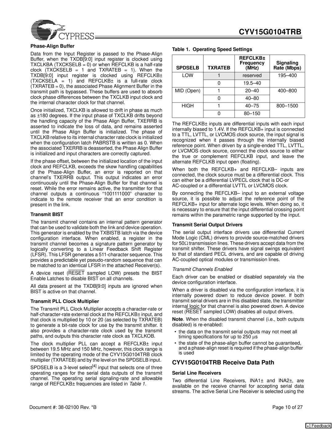
Table 1. Operating Speed Settings |
| ||
|
| REFCLKB± | Signaling |
SPDSELB | TXRATEB | Frequency | |
(MHz) | Rate (Mbps) | ||
LOW | 1 | reserved | |
| 0 |
| |
MID (Open) | 1 | ||
| 0 |
| |
HIGH | 1 | ||
| 0 |
| |
The REFCLKB± inputs are differential inputs with each input internally biased to 1.4V. If the REFCLKB+ input is connected to a TTL, LVTTL, or LVCMOS clock source, the input signal is recognized when it passes through the internally biased reference point. When driven by a
When both the REFCLKB+ and REFCLKB– inputs are connected, the clock source must be a differential clock. This can either be a differential LVPECL clock that is
By connecting the REFCLKB– input to an external voltage source, it is possible to adjust the reference point of the REFCLKB+ input for alternate logic levels. When doing so, it is necessary to ensure that the input differential crossing point remains within the parametric range supported by the input.
Transmit Serial Output Drivers
The serial output interface drivers use differential Current Mode Logic (CML) drivers to provide
Transmit Channels Enabled
Each driver can be enabled or disabled separately via the device configuration interface.
When a driver is disabled via the configuration interface, it is internally powered down to reduce device power. If both transmit serial drivers are in this disabled state, the transmitter internal logic for that channel is also powered down. A device reset (RESET sampled LOW) disables all output drivers.
Note. When the disabled transmit channel (i.e., both outputs disabled) is
•the data on the transmit serial outputs may not meet all timing specifications for up to 250 ∝s
•the state of the
CYV15G0104TRB Receive Data Path
Serial Line Receivers
Two differential Line Receivers, INA1± and INA2±, are available on the receive channel for accepting serial data streams. The active Serial Line Receiver is selected using the
Page 10 of 27
[+] Feedback