CYV15G0104TRB
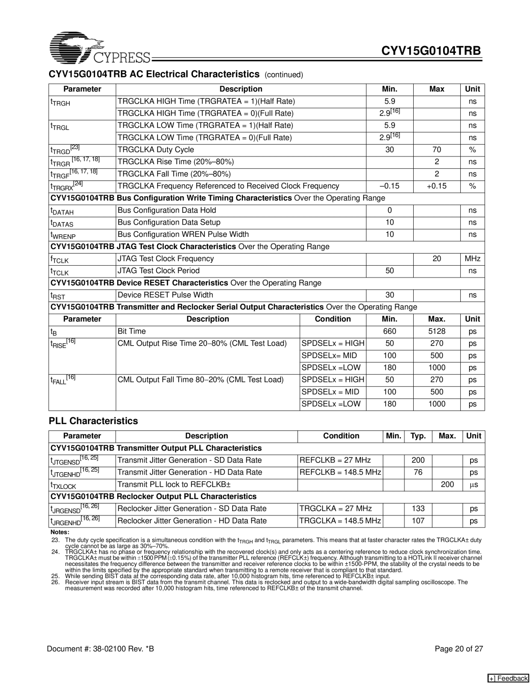
CYV15G0104TRB AC Electrical Characteristics (continued)
Parameter | Description |
| Min. | Max | Unit |
tTRGH | TRGCLKA HIGH Time (TRGRATEA = 1)(Half Rate) |
| 5.9 |
| ns |
| TRGCLKA HIGH Time (TRGRATEA = 0)(Full Rate) |
| 2.9[16] |
| ns |
tTRGL | TRGCLKA LOW Time (TRGRATEA = 1)(Half Rate) |
| 5.9 |
| ns |
| TRGCLKA LOW Time (TRGRATEA = 0)(Full Rate) |
| 2.9[16] |
| ns |
tTRGD[23] | TRGCLKA Duty Cycle |
| 30 | 70 | % |
tTRGR [16, 17, 18] | TRGCLKA Rise Time |
|
| 2 | ns |
tTRGF[16, 17, 18] | TRGCLKA Fall Time |
|
| 2 | ns |
tTRGRX[24] | TRGCLKA Frequency Referenced to Received Clock Frequency | +0.15 | % | ||
CYV15G0104TRB Bus Configuration Write Timing Characteristics Over the Operating Range |
|
| |||
tDATAH | Bus Configuration Data Hold |
| 0 |
| ns |
tDATAS | Bus Configuration Data Setup |
| 10 |
| ns |
tWRENP | Bus Configuration WREN Pulse Width |
| 10 |
| ns |
CYV15G0104TRB JTAG Test Clock Characteristics Over the Operating Range |
|
|
| ||
fTCLK | JTAG Test Clock Frequency |
|
| 20 | MHz |
tTCLK | JTAG Test Clock Period |
| 50 |
| ns |
CYV15G0104TRB Device RESET Characteristics Over the Operating Range |
|
|
| ||
tRST | Device RESET Pulse Width |
| 30 |
| ns |
CYV15G0104TRB Transmitter and Reclocker Serial Output Characteristics Over the Operating Range |
|
| |||
Parameter | Description | Condition | Min. | Max. | Unit |
tB | Bit Time |
| 660 | 5128 | ps |
tRISE[16] | CML Output Rise Time 20−80% (CML Test Load) | SPDSELx = HIGH | 50 | 270 | ps |
|
| SPDSELx= MID | 100 | 500 | ps |
|
| SPDSELx =LOW | 180 | 1000 | ps |
tFALL[16] | CML Output Fall Time 80−20% (CML Test Load) | SPDSELx = HIGH | 50 | 270 | ps |
|
| SPDSELx = MID | 100 | 500 | ps |
|
| SPDSELx =LOW | 180 | 1000 | ps |
PLL Characteristics
Parameter | Description | Condition | Min. Typ. | Max. Unit |
CYV15G0104TRB Transmitter Output PLL Characteristics
tJTGENSD[16, 25] tJTGENHD[16, 25]
tTXLOCK
Transmit Jitter Generation - SD Data Rate | REFCLKB = 27 MHz | 200 |
| ps |
Transmit Jitter Generation - HD Data Rate | REFCLKB = 148.5 MHz | 76 |
| ps |
Transmit PLL lock to REFCLKB± |
|
| 200 | ∝s |
CYV15G0104TRB Reclocker Output PLL Characteristics |
|
|
| |
tJRGENSD[16, 26] | Reclocker Jitter Generation - SD Data Rate | TRGCLKA = 27 MHz | 133 | ps |
tJRGENHD[16, 26] | Reclocker Jitter Generation - HD Data Rate | TRGCLKA = 148.5 MHz | 107 | ps |
Notes:
23.The duty cycle specification is a simultaneous condition with the tTRGH and tTRGL parameters. This means that at faster character rates the TRGCLKA± duty cycle cannot be as large as
24.TRGCLKA± has no phase or frequency relationship with the recovered clock(s) and only acts as a centering reference to reduce clock synchronization time. TRGCLKA± must be within ±1500 PPM (±0.15%) of the transmitter PLL reference (REFCLK±) frequency. Although transmitting to a HOTLink II receiver channel necessitates the frequency difference between the transmitter and receiver reference clocks to be within
25.While sending BIST data at the corresponding data rate, after 10,000 histogram hits, time referenced to REFCLKB± input.
26.Receiver input stream is BIST data from the transmit channel. This data is reclocked and output to a
Document #: | Page 20 of 27 |
[+] Feedback