CYV15G0104TRB
Pin Definitions (continued)
CYV15G0104TRB HOTLink II Serializer and Reclocking Deserializer
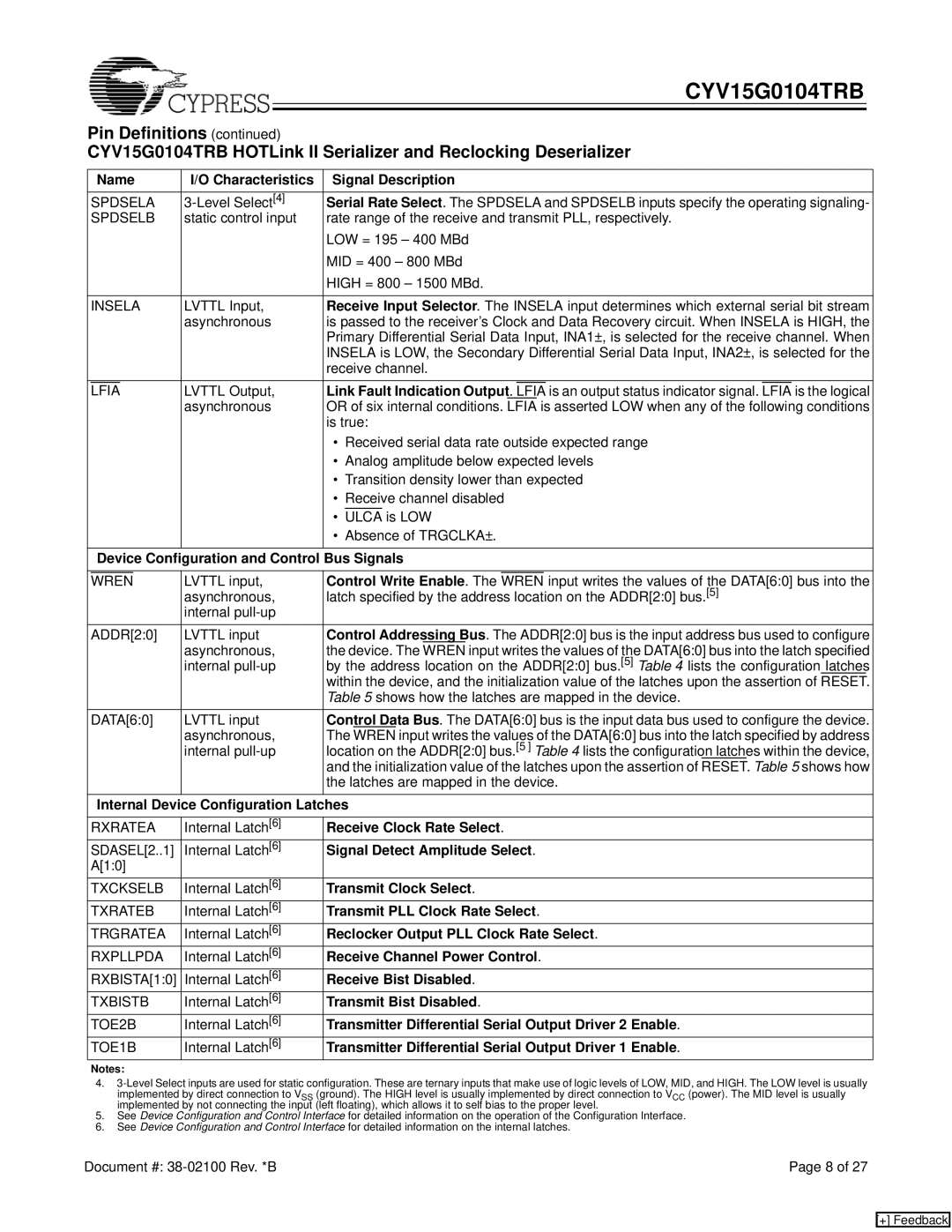
Name | I/O Characteristics | Signal Description |
SPDSELA | Serial Rate Select. The SPDSELA and SPDSELB inputs specify the operating signaling- | |
SPDSELB | static control input | rate range of the receive and transmit PLL, respectively. |
|
| LOW = 195 – 400 MBd |
|
| MID = 400 – 800 MBd |
|
| HIGH = 800 – 1500 MBd. |
INSELA | LVTTL Input, | Receive Input Selector. The INSELA input determines which external serial bit stream |
| asynchronous | is passed to the receiver’s Clock and Data Recovery circuit. When INSELA is HIGH, the |
|
| Primary Differential Serial Data Input, INA1±, is selected for the receive channel. When |
|
| INSELA is LOW, the Secondary Differential Serial Data Input, INA2±, is selected for the |
|
| receive channel. |
LFIA | LVTTL Output, | Link Fault Indication Output. LFIA is an output status indicator signal. LFIA is the logical |
| asynchronous | OR of six internal conditions. LFIA is asserted LOW when any of the following conditions |
|
| is true: |
|
| • Received serial data rate outside expected range |
|
| • Analog amplitude below expected levels |
|
| • Transition density lower than expected |
|
| • Receive channel disabled |
|
| • ULCA is LOW |
|
| • Absence of TRGCLKA±. |
Device Configuration and Control Bus Signals
WREN | LVTTL input, | Control Write Enable. The WREN input writes the values of the DATA[6:0] bus into the |
| asynchronous, | latch specified by the address location on the ADDR[2:0] bus.[5] |
| internal |
|
ADDR[2:0] | LVTTL input | Control Addressing Bus. The ADDR[2:0] bus is the input address bus used to configure |
| asynchronous, | the device. The WREN input writes the values of the DATA[6:0] bus into the latch specified |
| internal | by the address location on the ADDR[2:0] bus.[5] Table 4 lists the configuration latches |
|
| within the device, and the initialization value of the latches upon the assertion of RESET. |
|
| Table 5 shows how the latches are mapped in the device. |
DATA[6:0] | LVTTL input | Control Data Bus. The DATA[6:0] bus is the input data bus used to configure the device. |
| asynchronous, | The WREN input writes the values of the DATA[6:0] bus into the latch specified by address |
| internal | location on the ADDR[2:0] bus.[5 ] Table 4 lists the configuration latches within the device, |
|
| and the initialization value of the latches upon the assertion of RESET. Table 5 shows how |
|
| the latches are mapped in the device. |
Internal Device Configuration Latches | ||
RXRATEA | Internal Latch[6] | Receive Clock Rate Select. |
SDASEL[2..1] | Internal Latch[6] | Signal Detect Amplitude Select. |
A[1:0] |
|
|
TXCKSELB | Internal Latch[6] | Transmit Clock Select. |
TXRATEB | Internal Latch[6] | Transmit PLL Clock Rate Select. |
TRGRATEA | Internal Latch[6] | Reclocker Output PLL Clock Rate Select. |
RXPLLPDA | Internal Latch[6] | Receive Channel Power Control. |
RXBISTA[1:0] | Internal Latch[6] | Receive Bist Disabled. |
TXBISTB | Internal Latch[6] | Transmit Bist Disabled. |
TOE2B | Internal Latch[6] | Transmitter Differential Serial Output Driver 2 Enable. |
TOE1B | Internal Latch[6] | Transmitter Differential Serial Output Driver 1 Enable. |
Notes:
4.
5.See Device Configuration and Control Interface for detailed information on the operation of the Configuration Interface.
6.See Device Configuration and Control Interface for detailed information on the internal latches.
Document #: | Page 8 of 27 |
[+] Feedback