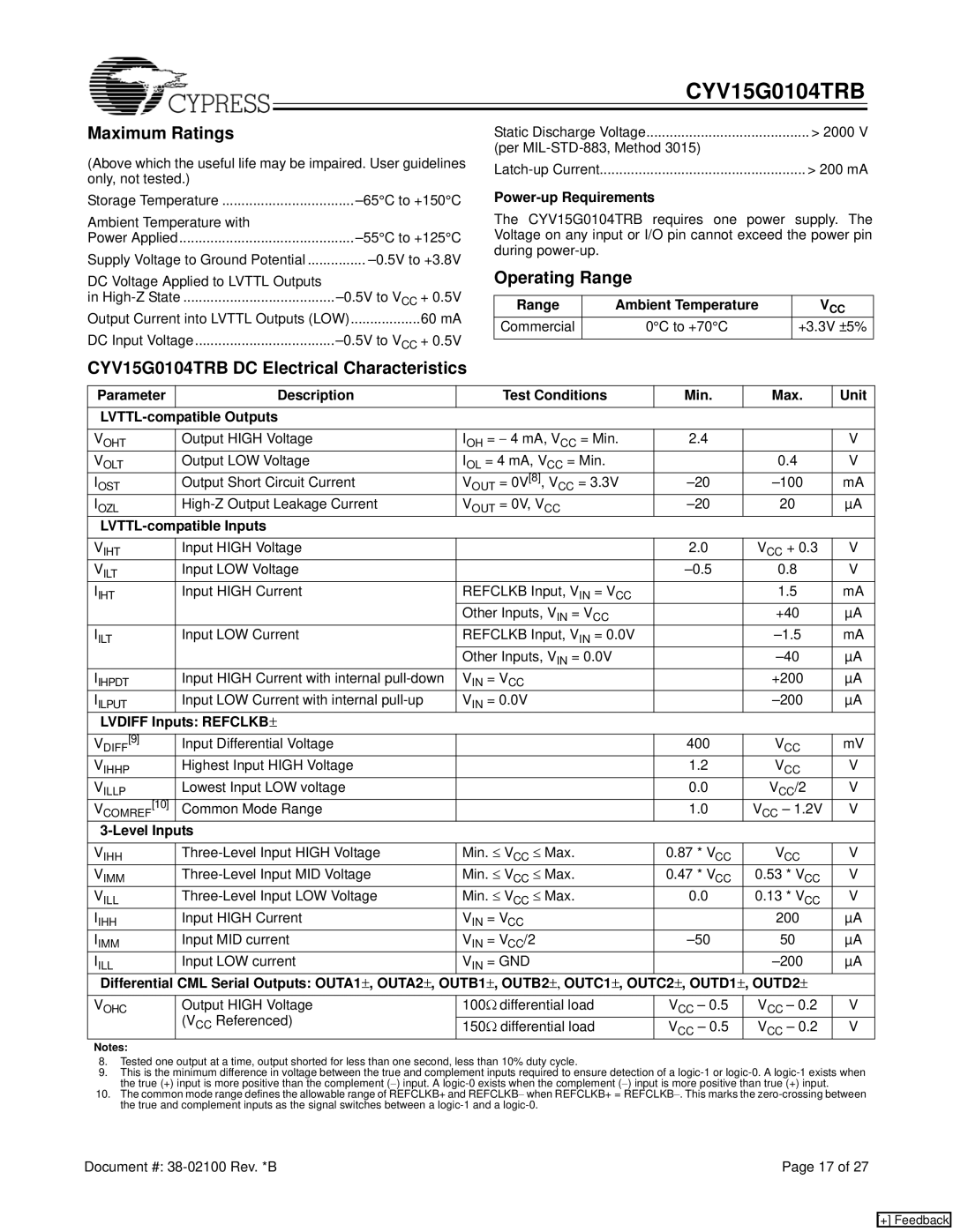
Maximum Ratings
(Above which the useful life may be impaired. User guidelines only, not tested.)
Storage Temperature | |
Ambient Temperature with |
|
Power Applied | |
Supply Voltage to Ground Potential |
| CYV15G0104TRB |
Static Discharge Voltage | .......................................... > 2000 V |
(per | |
> 200 mA | |
Power-up Requirements
The CYV15G0104TRB requires one power supply. The Voltage on any input or I/O pin cannot exceed the power pin during
DC Voltage Applied to LVTTL Outputs | Operating Range |
|
|
|
| |||
in | Range | Ambient Temperature | VCC | |||||
Output Current into LVTTL Outputs (LOW)..................60 mA | ||||||||
Commercial |
| 0°C to +70°C | +3.3V ±5% | |||||
DC Input |
| |||||||
|
|
|
|
|
| |||
CYV15G0104TRB DC Electrical Characteristics |
|
|
|
|
| |||
Parameter | Description | Test Conditions |
| Min. | Max. |
| Unit | |
|
|
|
|
|
| |||
VOHT | Output HIGH Voltage | IOH = − 4 mA, VCC = Min. | 2.4 |
|
| V | ||
VOLT | Output LOW Voltage | IOL = 4 mA, VCC = Min. |
|
| 0.4 |
| V | |
IOST | Output Short Circuit Current | VOUT = 0V[8], VCC = 3.3V |
| mA | ||||
IOZL | VOUT = 0V, VCC |
| 20 |
| µA | |||
|
|
|
|
|
|
| ||
VIHT | Input HIGH Voltage |
|
| 2.0 | VCC + 0.3 |
| V | |
VILT | Input LOW Voltage |
|
| 0.8 |
| V | ||
IIHT | Input HIGH Current | REFCLKB Input, VIN = VCC |
| 1.5 |
| mA | ||
|
| Other Inputs, VIN = VCC |
|
| +40 |
| µA | |
IILT | Input LOW Current | REFCLKB Input, VIN = 0.0V |
|
| mA | |||
|
| Other Inputs, VIN = 0.0V |
|
|
| µA | ||
IIHPDT | Input HIGH Current with internal | VIN = VCC |
|
| +200 |
| µA | |
IILPUT | Input LOW Current with internal | VIN = 0.0V |
|
|
| µA | ||
LVDIFF Inputs: REFCLKB± |
|
|
|
|
|
| ||
VDIFF[9] | Input Differential Voltage |
|
| 400 | VCC |
| mV | |
VIHHP | Highest Input HIGH Voltage |
|
| 1.2 | VCC |
| V | |
VILLP | Lowest Input LOW voltage |
|
| 0.0 | VCC/2 |
| V | |
VCOMREF[10] | Common Mode Range |
|
| 1.0 | VCC – 1.2V | V | ||
|
|
|
|
|
|
| ||
VIHH | Min. ≤ VCC ≤ Max. |
| 0.87 * VCC | VCC |
| V | ||
VIMM | Min. ≤ VCC ≤ Max. |
| 0.47 * VCC | 0.53 * VCC | V | |||
VILL | Min. ≤ VCC ≤ Max. |
| 0.0 | 0.13 * VCC | V | |||
IIHH | Input HIGH Current | VIN = VCC |
|
| 200 |
| µA | |
IIMM | Input MID current | VIN = VCC/2 |
| 50 |
| µA | ||
IILL | Input LOW current | VIN = GND |
|
|
| µA | ||
Differential CML Serial Outputs: OUTA1±, OUTA2±, OUTB1±, OUTB2±, OUTC1±, OUTC2±, OUTD1±, OUTD2± |
|
| ||||||
VOHC | Output HIGH Voltage | 100Ω differential load |
| VCC – 0.5 | VCC – 0.2 |
| V | |
| (VCC Referenced) | Ω |
| VCC – 0.5 | VCC – 0.2 |
| V | |
|
| 150 differential load |
|
| ||||
Notes:
8.Tested one output at a time, output shorted for less than one second, less than 10% duty cycle.
9.This is the minimum difference in voltage between the true and complement inputs required to ensure detection of a
the true (+) input is more positive than the complement (−) input. A
10.The common mode range defines the allowable range of REFCLKB+ and REFCLKB− when REFCLKB+ = REFCLKB−. This marks the
Document #: | Page 17 of 27 |
[+] Feedback