6806800E08A
Installation and Use
MVME7100 Single Board Computer
November
Contact Address
Trademarks
Limited and Restricted Rights Legend
2 Hardware Preparation and Installation
Contents
About this Manual Safety Notes Sicherheitshinweise 1 Introduction
3 Controls, LEDs, and Connectors
4 Functional Description
6 MOTLoad Firmware
A Battery Exchange
5 Transition Module
Contents
Related Specifications
MVME7100 Single Board Computer Installation and Use 6806800E08A
B Related Documentation
List of Tables
Emerson Network Power - Embedded Computing Publications
MVME7100 Single Board Computer Installation and Use 6806800E08A
Table B-1
MVME7100 Single Board Computer Installation and Use 6806800E08A
List of Tables
List of Figures
MVME7100 Single Board Computer Installation and Use 6806800E08A
Secondary Side Thermally Significant Components
Figure A-1
MVME7100 Single Board Computer Installation and Use 6806800E08A
List of Figures
Overview of Contents
About this Manual
Abbreviations
MVME7100 Single Board Computer Installation and Use 6806800E08A
About this Manual
TERM
MVME7100 Single Board Computer Installation and Use 6806800E08A
About this Manual
TERM
MEANING
MVME7100 Single Board Computer Installation and Use 6806800E08A
About this Manual
TERM
MEANING
Conventions
MVME7100 Single Board Computer Installation and Use 6806800E08A
About this Manual
Notation
Summary of Changes
Comments and Suggestions
Safety Notes
Safety Notes
MVME7100 Single Board Computer Installation and Use 6806800E08A
Installation
Operation
Cabling and Connectors
Battery
Sicherheitshinweise
Betrieb
Kabel und Stecker
Installation
Batterie
Umweltschutz
1.1 Features
Introduction
Table 1-1 Features List
Features
Table 1-1 Features List continued
IntroductionFeatures
Features
MVME7100 Single Board Computer Installation and Use 6806800E08A
1.2 Standard Compliances
1.3 Mechanical Data
Characteristic
MVME7100 Single Board Computer Installation and Use 6806800E08A
1.4.2 Board Accessories
1.4 Ordering Information
1.4.1 Supported Board Models
Table 1-4 Board Variants
Table 2-1 Startup Overview
Hardware Preparation and Installation
2.1 Overview
2.2 Unpacking and Inspecting the Board
Shipment Inspection
Table 2-2 MVME7100 Specifications
2.3 Requirements
2.3.1 Environmental Requirements
2.3.2 Power Requirements
Table 2-3 Power Requirements
Table 2-4 Thermally Significant Components
2.3.3 Thermal Requirements
2.3.4 Thermally Significant Components
Hardware Preparation and Installation
MVME7100 Single Board Computer Installation and Use 6806800E08A
Figure 2-1 Primary Side Thermally Significant Components
Figure 2-2 Secondary Side Thermally Significant Components
2.3.5 Equipment Requirements
z Transition module and connecting cables
Hardware Preparation and Installation
MVME7100 Single Board Computer Installation and Use 6806800E08A
Figure 2-3 Switch Locations
2.4 Configuring the Board
S1 S2
Table 2-5 Configuration Switch Settings S1
2.4.1 SMT Configuration Switch, S1
Figure 2-4 SMT Configuration Switch Position
2.4.1.1 Safe Start Switch
2.4.1.2 Boot Block B Select
2.4.1.3 Flash Bank Write Protect
2.4.1.4 JTAG Pass-Thru
2.4.2 Geographical Address Switch, S2
2.4.3 VME System Controller Select, S2
2.4.1.7 Master WP
Figure 2-5 Geographical Address Switch Position
Table 2-6 VME System Controller and GA Switch Settings continued
2.5 Installing Accessories
2.5.1 Transition Module
Installation and Removal Procedure
2.5.2 PMC
Installation Procedure
Figure 2-6 Typical Placement of a PMC Module on a VME Module
2.6 Installing and Removing the Board
2.5.3 XMCspan
Installation and Removal Procedure
2. Remove any filler panel that might fill that slot
MVME7100 bmw -af8000000 -bf8f00000 -c4000000 MVME7100 execP -l4000400
2.7 Completing the Installation
2.8 Factory Installed Linux
Login as root
Controls, LEDs, and Connectors
3.1 Overview
3.2 Board Layout
Battery J3 J2 J4A/J4B
Figure 3-2 Front Panel LEDs, Connectors, Switch
3.3.1 Reset/Abort Switch
3.3 Front Panel
3.3.2 LEDs
Controls, LEDs, and Connectors
MVME7100 Single Board Computer Installation and Use 6806800E08A
Table 3-1 Front Panel LEDs
3.3.3 Connectors
Table 3-2 Baseboard Connectors
3.3.3.1 XMC Expansion Connector J6
Table 3-3 XMC Expansion Connector J6 Pin Assignments
Connectors
Controls, LEDs, and Connectors
Table 3-4 Ethernet Connectors J4A/J4B Pin Assignments
3.3.3.2 Ethernet Connectors J4A/J4B
Table 3-3 XMC Expansion Connector J6 Pin Assignments continued
Table 3-5 PMC Slot 1 Connector J11 Pin Assignments
3.3.3.3 PCI Mezzanine Card PMC Connectors J11 - J14, J21 - J23
Table 3-4 Ethernet Connectors J4A/J4B Pin Assignments continued
Table 3-5 PMC Slot 1 Connector J11 Pin Assignments continued
Table 3-6 PMC Slot 1 Connector J12 Pin Assignments
Controls, LEDs, and ConnectorsConnectors
Signal
Table 3-6 PMC Slot 1 Connector J12 Pin Assignments continued
Table 3-7 PMC Slot 1 Connector J13 Pin Assignments
ConnectorsControls, LEDs, and Connectors
Signal
Table 3-7 PMC Slot 1 Connector J13 Pin Assignments continued
Table 3-8 PMC Slot 1 Connector J14 Pin Assignments
Controls, LEDs, and ConnectorsConnectors
Signal
Table 3-8 PMC Slot 1 Connector J14 Pin Assignments continued
Table 3-9 PMC Slot 2 Connector J21 Pin Assignments
ConnectorsControls, LEDs, and Connectors
Signal
Table 3-9 PMC Slot 2 Connector J21 Pin Assignments continued
Table 3-10 PMC Slot 2 Connector J22 Pin Assignments
Controls, LEDs, and ConnectorsConnectors
Signal
Table 3-10 PMC Slot 2 Connector J22 Pin Assignments continued
Table 3-11 PMC Slot 2 Connector J23 Pin Assignments
ConnectorsControls, LEDs, and Connectors
Signal
3.3.3.4 Serial Port Connector COM1/J1
3.3.3.5 VMEbus P1 Connector
Table 3-11 PMC Slot 2 Connector J23 Pin Assignments continued
Table 3-12 COM1 Port Connector Pin Assignments
3.3.3.6 VMEbus P2 Connector
Table 3-13 VMEbus P1 Connector Pin Assignments continued
Table 3-14 VME P2 Connector Pinouts
ConnectorsControls, LEDs, and Connectors
Table 3-14 VME P2 Connector Pinouts continued
Controls, LEDs, and ConnectorsConnectors
MVME7100 Single Board Computer Installation and Use 6806800E08A
P2-Z
3.3.3.7 MVME7216E PMC I/O Module PIM Connectors J10, J14
Table 3-15 MVME721 Host I/O Connector J10 Pin Assignments
3.3.3.8 USB Connector J2
3.4 Headers
3.4.1 Processor COP Header P4
Table 3-15 MVME721 Host I/O Connector J10 Pin Assignments continued
3.4.2 Boundary Scan Header P5
Table 3-18 Boundary Scan Header P5 Pin Assignments
Boundary Scan Header P5
Controls, LEDs, and Connectors
MVME7100 Single Board Computer Installation and Use 6806800E08A
Functional Description
4.1 Overview
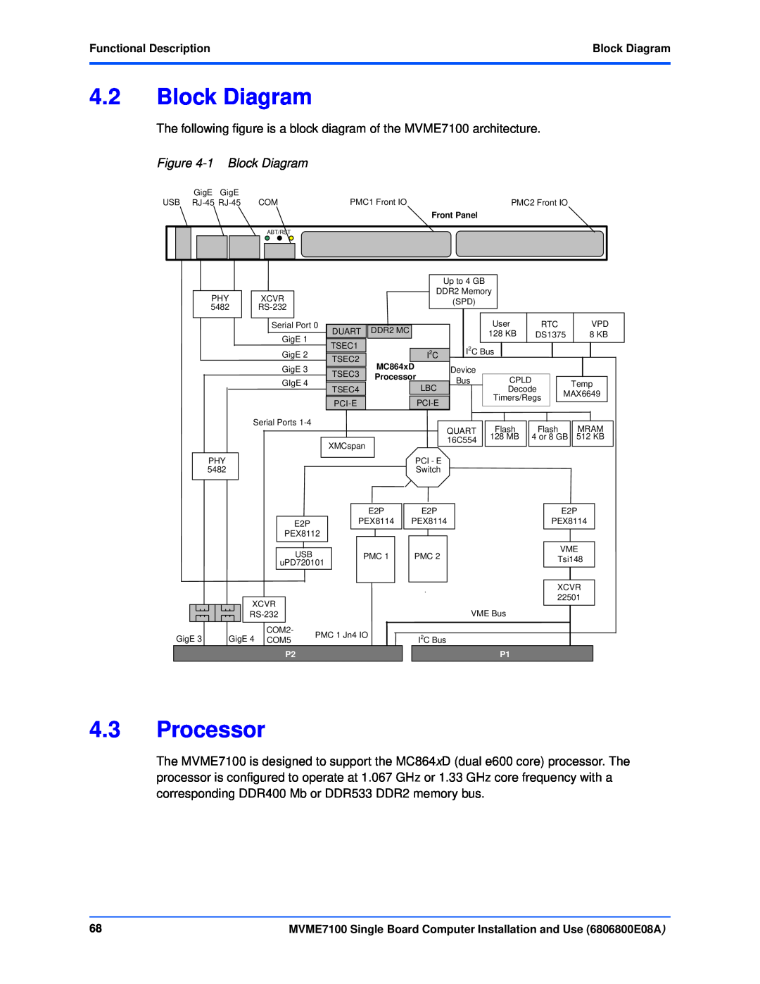
Figure 4-1 Block Diagram
4.2 Block Diagram
4.3 Processor
4.4 I2C Serial Interface and Devices
4.5 System Memory
4.6 Timers
4.7 Ethernet Interfaces
4.8 Local Bus Interface
Timers
4.8.4 Control and Timers PLD
4.8.1 Flash Memory
4.8.2 NVRAM
4.8.3 Quad UART QUART
4.9 DUART Interface
4.10 PCI-E Port
4.10.1 VME Controller
4.10.2 USB
4.12 Power Supplies
4.12.1 Power Sequencing
4.12.2 Power Supply Monitor
4.12.3 Power Supply Filtering and Fusing
4.14 Reset Control Logic
4.15 Real Time Clock Battery
4.13.1 System Clock
4.13.2 Real Time Clock Input
Transition Module
5.1 Overview
5.2 Transition Module Layout
Figure 5-1 Component Layout
5.3 Features
5.4 SEEPROM Address Switch, S1
Table 5-1 Transition Module Features
Figure 5-2 Block Diagram
5.5 Rear Panel Connectors
Table 5-2 SEEPROM Address Switch Assignments RTM
Table 5-3 Switch Settings and Device Addresses
Table 5-4 Transition Module Connectors
Figure 5-4 Rear Panel Connectors and LEDs
Rear Panel Connectors
MVME7100 Single Board Computer Installation and Use 6806800E08A
Table 5-5 Transition Module LEDs
Procedure
5.6 PMC Input/Output Module
Figure 5-5 Installing the PIM
MVME7100 Single Board Computer Installation and Use 6806800E08A
Transition Module
PMC Input/Output Module
6.3 MOTLoad Commands
MOTLoad Firmware
6.1 Overview
6.2 Implementation and Memory Requirements
6.3.2 Tests
Tests
6.3.3 Command List
Table 6-1 MOTLoad Commands
Command List
Command
Table 6-1 MOTLoad Commands continued
MOTLoad FirmwareCommand List
Command
MVME7100 Single Board Computer Installation and Use 6806800E08A
Table 6-1 MOTLoad Commands continued
Command ListMOTLoad Firmware
Command
MVME7100 Single Board Computer Installation and Use 6806800E08A
6.4 Using the Command Line Interface
Table 6-1 MOTLoad Commands continued
MOTLoad FirmwareUsing the Command Line Interface
Command
Example
6.4.1 Rules
6.4.2 Help
help commandname
MVME7100 flashProgram -d/dev/flash0 -n00100000
6.5 Firmware Settings
6.5.1 Default VME Settings
z MVME7100 vmeCfg -s -m
z MVME7100 vmeCfg -s -r234
z MVME7100 vmeCfg -s -o2
z MVME7100 vmeCfg -s
z MVME7100 vmeCfg -s -o1
z MVME7100 vmeCfg -s -o3
z MVME7100 vmeCfg -s -o7
6.5.4 Editing VME Settings
6.5.2 Control Register/Control Status Register Settings
6.5.3 Displaying VME Settings
6.5.5 Deleting VME Settings
6.5.6 Restoring Default VME Settings
6.6 Remote Start
vmeCfg -z
6.7 Boot Images
Table 6-2 MOTLoad Image Flags
6.7.1 Checksum Algorithm
6.7.2 Image Flags
6.7.3 User Images
6.7.6 Boot Image Firmware Scan
6.7.4 Alternate Boot Data Structure
6.7.5 Alternate Boot Images and Safe Start
6.8 Startup Sequence
Battery Exchange
A.1 Battery Exchange
Battery
Figure A-1 Battery Location
2. Install the new battery with the plus sign + facing up
Exchange Procedure
1. Remove the old battery
B.1 Emerson Network Power - Embedded Computing Documents
Related Documentation
B.2 Manufacturers’ Documents
Table B-1 Emerson Network Power - Embedded Computing Publications
MVME7100 Single Board Computer Installation and Use 6806800E08A
Table B-2 Manufacturer’s Publications continued
Related DocumentationManufacturers’ Documents
Document Title and Source
B.3 Related Specifications
Table B-3 Related Specifications
Related SpecificationsRelated Documentation
MVME7100 Single Board Computer Installation and Use 6806800E08A
Table B-3 Related Specifications continued
Related DocumentationRelated Specifications
MVME7100 Single Board Computer Installation and Use 6806800E08A
Organization and Standard
Index
MVME7100 Single Board Computer Installation and Use 6806800E08A