
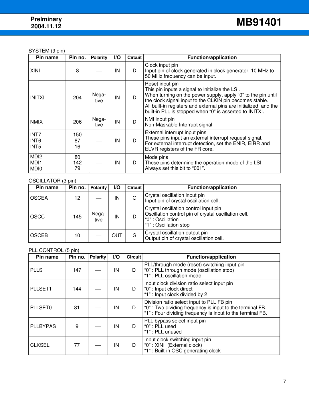
MB91401 specifications
The Fujitsu MB91401 microcontroller is a versatile device designed for automotive applications, embedded systems, and industrial control. It belongs to the MB91400 series, known for its robustness and efficiency. This series integrates advanced features and technologies that cater to a wide variety of real-time applications.One of the standout features of the MB91401 is its 32-bit RISC architecture, which operates at clock speeds up to 40 MHz. This high-performance core enables rapid processing and data handling, making it suitable for demanding applications. The microcontroller is equipped with a generous amount of Flash memory, allowing developers to store essential firmware and applications directly on the chip, enhancing reliability and reducing design complexity.
Another key characteristic is its extensive memory configuration, which includes SRAM for data storage and EEPROM for non-volatile data retention. This combination provides flexibility for developers, enabling them to tailor the memory allocation based on specific application requirements.
The MB91401 is designed with a focus on peripheral integration. It features multiple I/O ports, timer units, and A/D converters, making it an ideal choice for applications that require precise timing and analog signal processing. The analog-to-digital converters offer high resolution and fast conversion speeds, which are critical in automotive and industrial control systems where accuracy is paramount.
Safety is a critical consideration in automotive applications, and the MB91401 addresses this with built-in diagnostic features and error detection capabilities. These features help ensure that the application remains functional and safe under various operating conditions.
In terms of connectivity, the microcontroller supports various communication protocols, including CAN, UART, and SPI, facilitating seamless integration with other systems and devices. This is particularly important in automotive applications where communication between different electronic control units (ECUs) is essential for overall system functionality.
The Fujitsu MB91401 is also designed for low power consumption, making it suitable for battery-operated devices and energy-sensitive applications. Its various power-saving modes allow developers to optimize the system's performance while extending operational life.
In summary, the Fujitsu MB91401 is a powerful and flexible microcontroller that combines high-performance processing with extensive peripheral support and safety features. Its robust architecture and energy-efficient design make it an excellent choice for a wide range of automotive and industrial applications, promoting both reliability and innovation in embedded system development.