C156-E142-02EN
MCE3130AP, MCE3064AP MCF3064AP OPTICAL DISK DRIVES PRODUCT MANUAL
All Rights Reserved. Copyright ! 2001 FUJITSU LIMITED
The contents of this manual is subject to change without prior notice
REVISION RECORD
Revised contents
Edition
Date published
Chapter 3 INSTALLATION REQUIREMENTS
Chapter 2 SPECIFICATIONS
Chapter 5 OPERATION AND CLEANING
Chapter 6 DIAGNOSIS AND MAINTENANCE
Conventions for Alert Messages
C156-E142-02EN
DISCLAIMER
The surface temperatures of some ICs on the printed circuit board
Low temperature burns
Use an antistatic mat and wrist strap when handling the
Hold the mounting frame when handling the drive. Do
and enables you to insert the cartridge
Be sure to turn on the power supply before inserting your cartridge
turn on the power supply beforehand
1 Make sure that the system power is off
GENERAL DESCRIPTION SPECIFICATIONS INSTALLATION REQUIREMENTS
MCE3064AP and MCF3064AP OPTICAL DISK DRIVE MAINTENANCE MANUAL
HOST INTERFACE OPERATION AND CLEANING DIAGNOSIS AND MAINTENANCE
MAINTENANCE AND DIAGNOSIS FAULT ANALYSIS
Standards Institute
REFERENCED STANDARDS
SPECIFICATIONS
CONTENTS
INSTALLATION REQUIREMENTS
CHAPTER
CHAPTER
HOST INTERFACE
ATA Features register
Error register
ATAPI Features register
Reset response
SET FEATURES XEF
SERVICE XA2 Not supported
Packet Commands
ERASE command
CHAPTER 6 DIAGNOSIS AND MAINTENANCE
CHAPTER 5 OPERATION AND CLEANING
GLOSSARY
ABBREVIATIONS
FIGURES
Cleaning procedure
Cleaning procedure
Cleaning procedure
Cleaning procedure
TABLES
GET MEDIA STATUS command
EXECUTE DEVICE DIAGNOSTIC command
Error register
IDLE IMMEDIATE command
Removable block access capabilities page
Default values for the cashing page
Changeable values in the removable block access capabilities page
Default values for the removable block access capabilities page
SEEK command
SEND DIAGNOSTIC command
START/STOP UNIT command
SYNCHRONIZE CACHE command
CHAPTER 1 GENERAL DESCRIPTION
1.1 Features 1.2 Drive Configuration 1.3 System Configuration
1.1 Features
1.1.1 Performance
1.1.4 Adaptability
1.1.2 Reliability
1.1.3 Maintainability/operability
1.1.5 Interface
Page
Figure 1.1 Outer view with panel Figure 1.2 Outer view without panel
1.2 Drive Configuration 1.2.1 Drive model
Figures 1.1 and 1.2 show the outer view
C156-E142-02EN
Figure 1.3 Optical disk drive configuration 1.2.3 Mechanical sections
1.2.2 Configuration
1.2.4 Control circuit section
Figure 1.4 Control circuit section block diagram
1 ATAPI controller circuit section
Laser diode control circuit Signal reproduction circuit
2 Drive circuit section
The drive circuit section consists of the following circuits
Figure 1.6 System configuration with two optical disk drives
1.3 System Configuration
Figure 1.5 System configuration with one optical disk drive
2.1 Optical Disk Drive Specifications
CHAPTER 2 SPECIFICATIONS
2.2 Optical Disk Cartridge Specifications 2.3 Defect Management
2.1 Optical Disk Drive Specifications 2.1.1 Model and product number
C156-E142-02EN
Table 2.1 Model and order number 2 of
Table 2.2 Specifications 1 of
2.1.2 Drive specifications
Table 2.2 lists MCE3130AP, MCE3064AP, MCF3064AP drives specifications
MCE3130AP
C156-E142-02EN
Table 2.2 Specifications 2 of
MCE3064AP
C156-E142-02EN
Table 2.2 Specifications 3 of
MCF3064AP
Table 2.2 Specifications 4 of
No cartridge, power ON
2.1.3 Environmental and power requirements
Table 2.3 Environmental and power requirements 1 of
2.1.4 Error rate
Table 2.3 Environmental and power requirements 2 of
2.1.5 Reliability
Table 2.4 Recommended optical disk cartridge specifications
2.2 Optical Disk Cartridge Specifications
2.2.1 Recommended optical disk cartridge specifications
Figure 2.1 Optical disk cartridge
2.2.2 Optical disk cartridge
∃ Shutter closed 2 Shutter 1 Cartridge case 3 Write protect tab
∃ Shutter open
1 Cartridge case
The write protect tab selects whether write is enabled or disabled
2 Shutter
3 Write protect tab
Disk specifications
2.2.3 Disk specifications
Figure 2.2 Algorithms for alternate processing
2.3 Defect Management 2.3.1 Defect management schematic diagram
a Sector slipping algorithm b Linear replacement algorithm
C156-E142-02EN
Figure 2.3 Example of alternate processing
3.3 Power supply Requirements 3.4 Cable Connections
CHAPTER 3 INSTALLATION REQUIREMENTS
3.5 Jumper Settings 3.6 Notes on Drive Handling 3.7 Mounting
3.9 Operation Confirmation and Preparation for Use after Installation
a Inside optical disk cartridge Operating of inner partition wall
Figure 3.1 Surface temperature measurement points
Tip of thermocouple Hole for inserting thermocouple
b IC controller, read map
3.1.3 Air flow
3.1.2 Temperature requirements and measuring method
Table 3.1 Temperature requirements at measurement points
3.1.5 Air purity
3.1.4 Temperature rise under several conditions
Table 3.2 Temperature at each measuring point Reference
Figure 3.2 Dimensions
3.2 Mounting Requirements 3.2.1 External dimensions
Unit mm Note The height length is 25.4 ± 0.8 besides the panel size
C156-E142-02EN
C156-E142-02EN
Figure 3.3 Dimensions without panel
Unit mm Note Those enclosed in parentheses are inch screws
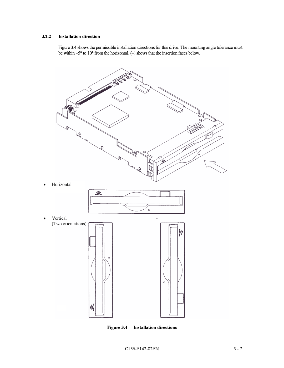
Figure 3.4 Installation directions
3.2.2 Installation direction
# Horizontal # Vertical Two orientations
C156-E142-02EN
Figure 3.5 Centers of gravity
3.2.3 Centers of gravity
Figure 3.5 shows the centers of gravity of the drive Unit mm
C156-E142-02EN
∃15 orless
3.2.4 Notes on mounting
Figure 3.6 Mounting frame structure
Figure 3.7 Service clearance
Figure 3.8 Current waveform +5 VDC
3.3 Power Supply Requirements
Figure 3.9 Connector and terminal locations
3.4 Cable Connections 3.4.1 Drive connectors
Table 3.3 Cable connector specifications
3.4.2 Cable connector specifications
Figure 3.10 Cable connection diagram
3.4.3 Drive connection
Figure 3.11 Jumper settings at factory shipping 3.5.2 Mode setting
3.5 Jumper Settings 3.5.1 Jumper settings at factory shipping
Figure 3.12 Master device setting
CNH15
CNH5CNH1
Figure 3.13 Slave device setting
Figure 3.14 Cable select mode setting
Figure 3.15 Cable select examples
3.6 Notes on Drive Handling
Use an antistatic mat and wrist strap when handling the drive
2 Do not leave the drive in dirty or contaminated environments
Device damage
Device damage
3 Installation
Figure 3.17 Gathered packaging style
Figure 3.16 Individual packaging style
Eject Pin %
Master carton 12/24 units
3.7 Mounting 3.7.1 Checks before mounting the drive
3.7.2 Mounting procedure
1 Make sure that the system power is off
2 Do not connect or disconnect any cable when the power is on
The BUSY LED is on while the optical disk drive is executing seek, write, or read operations. The BUSY LED is on momentarily, so it seems as if it blinked or is off
3.9.1 Confirming initial operations
3.9 Operation Confirmation and Preparation for Use after Installation
Device damage
3.9.2 Connection check
3.10 Dismounting Drive
4.4 Various Processes 4.5 ATA Commands 4.6 Packet Commands 4.7 Timing
4.1 Pin Assignment 4.2 Signal Description 4.3 Interface Registers
Table 4.1 Differences in Host Interface Specifications of Each Model
CHAPTER 4 HOST INTERFACE
4.1 Pin Assignment
Table 4.2 Connector pin assignments 1/2
Table 4.2 Connector pin assignments 2/2
4.2 Signal Description Table 4.3 Signal description
Table 4.4 I/O port functions and mapping
4.3 Interface Registers 4.3.1 I/O registers
4.3.1.1 Alternate Status register
4.3.1.2 ATA Command register
Table 4.5 Bit definitions of Alternate Status register
4.3.1.3 Data register
Table 4.7 Bit definitions of Drive Address register
4.3.1.5 Drive Address register
4.3.1.6 ATAPI Byte Count register
Table 4.8 Bit definitions of ATAPI Byte Count register
Table 4.10 Bit definitions of Error register
4.3.1.8 Error register
4.3.1.7 ATAPI Block Device Select register
Table 4.9 Bit definitions of ATAPI Block Device Select register
4.3.1.10 ATAPI Features register
4.3.1.9 ATA Features register
Table 4.11 Bit definitions of ATAPI Features register
4.3.1.11 ATA Sector Count register
4.3.1.13 Sector Number register
Table 4.13 IO and Cod
4.3.1.14 ATAPI Status register
Table 4.14 Bit definitions of ATAPI Status register
e During DMA transfer when the DRQ bit is not set
b Within 400 ns of receiving a command when the DRQ bit is not set
CHECK bit of the Status register Error register Device/Head register
In all other cases, the ODD does not set BSY
4.4 Various Processes 4.4.1 Reset response
Table 4.15 Alternate sector assignment criteria
4.4.2 Defect sector management
4.4.3 Automatic alternate sector assignment function
4.4.4 Data error detection criteria
4.4.5.2 Read cache
4.4.5 Cache function
4.4.5.1 Data buffer
4.4.5.3 MO write cache
4.4.6 Media status notification function
4.4.7 Power management function
4.4.7.2 Active mode
4.4.7.1 Power mode
4.4.7.3 Pre-idle mode
4.4.7.4 Idle mode
4.4.7.7 Standby timer
4.4.7.6 Sleep mode
4.4.7.8 Power mode transition
Figure 4.1 Power mode
Table 4.17 LED indications
4.4.8 LED Indications
Table 4.18 Command codes and parameters
4.5 ATA Commands
Protocol
code
4.5.1 IDENTIFY PACKET DEVICE XA1
Table 4.19 IDENTIFY PACKET DEVICE command
Table 4.20 Device parameter information 1/5
Table 4.20 Device parameter information 2/5
Table 4.20 Device parameter information 3/5
Table 4.20 Device parameter information 4/5
4.5.2 PACKET XA0
Table 4.21 PACKET command
Table 4.20 Device parameter information 5/5
Table 4.22 DEVICE RESET command
4.5.3 DEVICE RESET
4.5.4 CHECK POWER MODE X98/XE5
Table 4.23 CHECK POWER MODE command
4.5.5 EXECUTE DEVICE DIAGNOSTIC
Table 4.24 Power mode indication
Table 4.25 EXECUTE DEVICE DIAGNOSTIC command
When no device 1 is connected
Table 4.27 GET MEDIA STATUS command
When the ODD is device
Table 4.26 Self-diagnosis detailed code
4.5.6 GET MEDIA STATUS XDA
4.5.7 IDLE IMMEDIATE X95/XE1
Error register
Table 4.29 IDLE IMMEDIATE command
4.5.9 SERVICE XA2 Not supported
NOP command
SERVICE command
4.5.8 NOP
Table 4.33 FR register setting value
4.5.10 SET FEATURES XEF
Table 4.32 SET FEATURES command
Table 4.34 Transfer setting values in the SC register
Table 4.35 Cylinder High register
SLEEP command
4.5.11 SLEEP X99/XE6
PRVENAB
4.5.12 STANDBY IMMEDIATE X94/XE0
Table 4.37 STANDBY IMMEDIATE command
Table 4.38 Packet command codes and parameters
4.6 Packet Commands
4.6.1 Logical Unit Number
4.6.2 ERASE command
ERASE command
Table 4.42 Defect list header
4.6.3 FORMAT UNIT command Table 4.40 FORMAT UNIT command
Table 4.41 FORMAT UNIT parameter list
Format descriptor
4.6.4 INQUIRY command
INQUIRY command
Table 4.45 INQUIRY data
Table 4.47 Mode parameters
4.6.5 MODE SELECT command Table 4.46 MODE SELECT command
Page descriptor
Table 4.48 Mode parameter list
Table 4.49 Mode parameter header
Table 4.51 Drive operation mode page
4.6.5.1 Drive operation mode page
Table 4.52 Changeable values in drive operation mode page
Table 4.53 Default values for the drive operation mode page
Table 4.54 Read-Write error recovery page
4.6.5.2 Read-Write error recovery page
Table 4.56 Default values for the read-write recovery page
Table 4.55 Changeable values in the read-write recovery page
Table 4.57 Flexible disk page
4.6.5.3
Flexible disk page
Table 4.58 Changeable values in flexible disk page
Table 4.59 Default values in flexible disk page
4.6.5.4
Table 4.62 Default values for the cashing page
Caching page
Table 4.61 Changeable values in the caching page
Table 4.63 Removable block access capabilities page
4.6.5.5 Removable block access capabilities page
Table 4.67 Inactivity Time Multiplier value
4.6.5.6 Timer & protect page Table 4.66 Timer & protect page
Table 4.69 Default values for the timer & protect page
Table 4.68 Changeable values for the timer & protect page
Table 4.71 Page Control field
4.6.6 MODE SENSE command Table 4.70 MODE SENSE command
Table 4.72 Mode parameter list
Page descriptor
Table 4.73 Mode parameter header
Table 4.76 Response to Prevent/Allow/Eject
4.6.7 PREVENT/ALLOW MEDIUM REMOVAL command
Table 4.75 PREVENT/ALLOW MEDIUM REMOVAL command
READ command
4.6.8 READ 10 command
4.6.9 READ 12 command
READ command
Table 4.81 READ CAPACITY data PMI = 1, MO media, FROM media
4.6.10 READ CAPACITY command Table 4.79 READ CAPACITY command
Table 4.80 READ CAPACITY data PMI =
Table 4.83 READ FORMAT CAPACITIES command
4.6.11 READ FORMAT CAPACITIES command
Table 4.82 READ CAPACITY data PMI = 1, PROM media
Table 4.84 READ FORMAT CAPACITIES data format
Table 4.87 Descriptor code definition
4.6.12 READ DEFECT DATA command Table 4.88 READ DEFECT DATA command
Table 4.86 Current/Maximum capacity descriptor
Defect descriptor
Table 4.89 Defect list formats
Table 4.91 Defect list header
Physical sector address format
Table 4.93 RECEIVE DIAGNOSTIC RESULTS command
4.6.13 READ LONG command Table 4.92 READ LONG command
4.6.14 RECEIVE DIAGNOSTIC RESULTS command
Table 4.95 Request sense data
4.6.15 REQUEST SENSE command
REQUEST SENSE command
Table 4.97 Sense key
Table 4.96 Error code
Sense
Table 4.98 Logical block address format
Table 4.99 ASC/ASCQ list 1/2
Table 4.99 ASC/ASCQ list 2/2
Table 4.100 Format Progress Indication Bytes
4.6.16 SEND DIAGNOSTIC command Table 4.101 SEND DIAGNOSTIC command
START/STOP UNIT command
4.6.17 SEEK command Table 4.102 SEEK command
4.6.18 START/STOP UNIT command
Table 4.104 START/STOP/EJECT processing
4.6.19 SYNCHRONIZE CACHE command
Table 4.105 SYNCHRONIZE CACHE command
ByteChk
4.6.20 TEST UNIT READY command Table 4.106 TEST UNIT READY command
4.6.21 VERIFY command Table 4.107 VERIFY command
4.6.23 WRITE 12 command Table 4.109 WRITE 12 command
4.6.22 WRITE 10 command Table 4.108 WRITE 10 command
4.6.24 WRITE AND VERIFY command Table 4.110 WRITE AND VERIFY command
Valid download data is Fujitsu distributed data only
4.6.25 WRITE BUFFER command Table 4.111 WRITE BUFFER command
Table 4.112 Code-ID
Download procedure
4.6.26 WRITE LONG command Table 4.113 WRITE LONG command
Figure 4.2 Register/PIO data transfer
4.7 Timing 4.7.1 Register/PIO data transfer timing
t0 DA20 CS0-/CS1 t1 t2 t9 t2i DIOR-/DIOW WRITE DD150 t3 t4 READ
DD150 t5 t6
Table 4.114 Register/PIO data transfer timing parameters
Figure 4.3 Multiword DMA data transfer
4.7.2 Multiword DMA data transfer timing
Table 4.115 Multiword DMA data transfer timing parameters
Figure 4.4 Power-on and reset timing
4.7.3 Power-on and Reset Timing
Table 4.116 Power-on and reset timing
5.1 Operating Optical Disk Drive 5.2 Cleaning Drive
CHAPTER 5 OPERATION AND CLEANING
5.4 Cleaning Optical Disk Cartridge
5.3 Optical Disk Cartridge Operation
5.1.3 Inserting cartridge
5.1.2 Note
1 Make sure that no optical disk cartridge is in the disk drive
2 When the drive power is off
2 Keep the cartridge shutter surface upward
3 Insert the cartridge, shutter first, into the disk insertion slot
5.1.4 Ejecting removing cartridge
Figure 5.2 Inserting cartridge
C156-E142-02EN
Figure 5.3 Removing cartridge
Push the eject button
Head cleaner
5.2 Cleaning Drive
Be sure to use the dedicated head cleaner described above
Device Damage
Figure 5.4 Optial disk cartridge
5.3 Optical Disk Cartridge Operation 5.3.1 Optical disk cartridge
See Subsection 2.3.2 for the functions of the parts Shutter closed
2. Shutter 1. Cartridge case 3. Write protect tab Shutter open
Figure 5.5 Write protect tab
5.3.2 Write protect tab
Cleaning kit
5.4.1 Cleaning tool
5.3.3 Notes
5.4 Cleaning Optical Disk Cartridge
5.4.2 Cleaning procedure
Table 5.3 Packaged items cleaning kit
Damage for data medium
Setting case
Figure 5.6 Cleaning procedure
Put a disposable groves at cleaning not put on the disk media
Figure 5.7 Cleaning procedure
Damage for disk medium
Damage for disk medium
Figure 5.8 Cleaning procedure
Eye inflammation
In case of contact with eyes, immediately flush eyes with water
C156-E142-02EN
Figure 5.9 Cleaning procedure
7 Turn the revolving knob, then wipe the disk surface Cleaning cloth
6.1 Diagnosis 6.2 Maintenance Information
CHAPTER 6 DIAGNOSIS AND MAINTENANCE
Table 6.1 Self-diagnostic function
6.1 Diagnosis
6.1.3 Test program
6.1.2 Diagnostic command
6.1.1 Initial self-diagnosis
Data loss
6.2 Maintenance Information 6.2.1 Maintenance requirements
Figure 6.2 Revision number indication
6.2.2 Revision number
Figure 6.1 Revision label
CDB Command Descriptor Block
Axial displacement
Command
Error correction code
Status
Sense key
Spindle
Abbreviations
Synchronous Data Transfer Request
Index
Page
Page
I, Place des Etas-Unis, SILIC 310, 94588 Rungis Cedex, FRANCE
Reader Comment Form
FUJITSU LIMITED