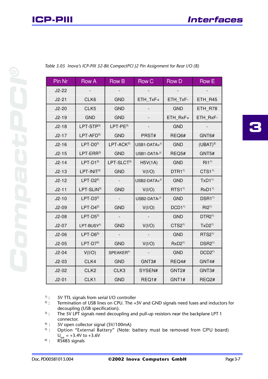
Table 3.05 Inova’s
®CompactPCI |
|
|
|
|
|
|
|
|
CLK2 | CLK3 | SYSEN# | GNT2# | GNT3# |
|
| ||
| Pin Nr | Row A | Row B | Row C | Row D | Row E |
|
|
| - | - | - | - | - |
|
| |
| CLK6 | GND | ETH_TxF+ | ETH_TxF- | ETH_R45 |
|
| |
| CLK5 | GND | - | GND | ETH_R78 |
|
| |
| GND | GND | - | ETH_RxF+ | ETH_RxF- |
| 3 | |
| - | GND | - |
| ||||
| GND | PRST# | REQ6# | GNT6# |
| |||
| GND | (UBAT)5) |
|
| ||||
| GND | REQ5# | GNT5# |
|
| |||
| H5V(1A) | GND | RI11) |
|
| |||
| GND | V(I/O) | DTR11) | CTS11) |
|
| ||
| - | GND | TxD11) |
|
| |||
| GND | V(I/O) | RTS11) | RxD11) |
|
| ||
| - | GND | DSR11) |
|
| |||
| GND | V(I/O) | DCD11) | RI21) |
|
| ||
| - | - | GND | DTR21) |
|
| ||
| GND | V(I/O) | CTS21) | TxD21) |
|
| ||
| - | - | GND | RTS21) |
|
| ||
| GND | V(I/O) | RxD21) | DSR21) |
|
| ||
| V(I/O) | SPEAKER4) | - | GND | DCD21) |
|
| |
| CLK4 | GND | GNT3# | REQ4# | GNT4# |
|
| |
|
|
|
|
|
|
|
|
|
| CLK1 | GND | REQ1# | GNT1# | REQ2# |
|
| |
|
|
|
|
|
|
|
|
|
1): 5V TTL signals from serial I/O controller
2): Termination of USB lines on CPU. The +5V and GND signals need fuses and inductors for decoupling (USB specification).
3): The 5V LPT signals need decoupling and
4): 5V open collector signal (5V/100mA)
5): Option “External Battery” (Note: battery must be removed from CPU board)
Ubat = +3.4V to +3.6V
6): RS485 signals
Doc. PD00581013.004 | ©2002 Inova Computers GmbH |