InterfacesICP-PIII
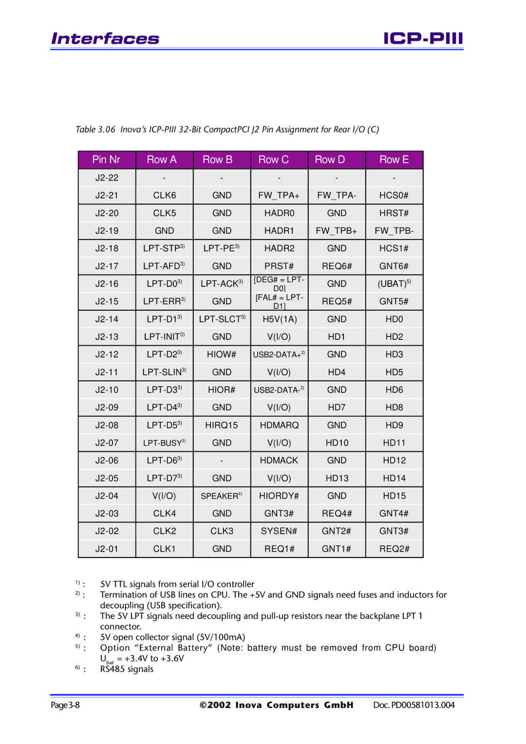
Table 3.06 Inova’s
Pin Nr | Row A | Row B | Row C | Row D | Row E |
|
|
|
|
|
|
- | - | - | - | - | |
CLK6 | GND | FW_TPA+ | FW_TPA- | HCS0# | |
|
|
|
|
|
|
CLK5 | GND | HADR0 | GND | HRST# | |
GND | GND | HADR1 | FW_TPB+ | FW_TPB- | |
|
|
|
|
|
|
HADR2 | GND | HCS1# | |||
GND | PRST# | REQ6# | GNT6# | ||
[DEG# = LPT- | GND | (UBAT)5) | |||
|
|
| D0] |
|
|
GND | [FAL# = LPT- | REQ5# | GNT5# | ||
|
|
| D1] |
|
|
H5V(1A) | GND | HD0 | |||
GND | V(I/O) | HD1 | HD2 | ||
HIOW# | GND | HD3 | |||
GND | V(I/O) | HD4 | HD5 | ||
HIOR# | GND | HD6 | |||
GND | V(I/O) | HD7 | HD8 | ||
HIRQ15 | HDMARQ | GND | HD9 | ||
GND | V(I/O) | HD10 | HD11 | ||
|
|
|
|
|
|
- | HDMACK | GND | HD12 | ||
GND | V(I/O) | HD13 | HD14 | ||
V(I/O) | SPEAKER4) | HIORDY# | GND | HD15 | |
CLK4 | GND | GNT3# | REQ4# | GNT4# | |
|
|
|
|
|
|
CLK2 | CLK3 | SYSEN# | GNT2# | GNT3# | |
CLK1 | GND | REQ1# | GNT1# | REQ2# | |
|
|
|
|
|
|
1): 5V TTL signals from serial I/O controller
2): Termination of USB lines on CPU. The +5V and GND signals need fuses and inductors for decoupling (USB specification).
3): The 5V LPT signals need decoupling and
4): 5V open collector signal (5V/100mA)
5): Option “External Battery” (Note: battery must be removed from CPU board)
Ubat = +3.4V to +3.6V
6): RS485 signals
©2002 Inova Computers GmbH | Doc. PD00581013.004 |