User’s Manual ECB-865
FCC Statement
Life Support Policy
Copyright Notice
Trademark Acknowledgement
Disclaimer
Evalue Technology Inc Evalue Europe A/S
Evalue Customer Services
Message to the Customer
Technical Support
Product Warranty
Packing List
Manual Objectives Introduction
Watchdog Timer Programming Jumper & Connector
Connector Definitions
Setting Jumpers
Entering Setup
Map
Revision Date Comment
Document Amendment History
Manual Objectives
System Overview
Introduction
Chipset ITE IT8712F-A
System Specifications
Expansion Interface
Mechanical and Environmental
Weight 0.5 Kg
Architecture Overview
1 82815 Gmch and 82801BA
Multiplexed AGP and Display Cache Interface
Dram Interface
AGP Interface
6 USB
PCI Interface
Ethernet 7.1 ICH2 LAN Controller
ITE IT8712F-A
Intel
Systems DiskOnChip
Installation Procedure
Hardware Configuration
Safety Precautions
Main Memory
Removing CPU
Expansion Interface Installing the Single Board Computer
Installing DOC
Systems’ DiskOnChip Flash Disk
1 815E integrated Graphics Controller
Drivers Support
Re-trigger WDT
Watchdog Timer Programming
Enable WDT
Disable WDT
Jumper & Connector Jumper & Connector Layout
JP11
Jumper & Connector List
Jumpers Label Function
JP10
J12
Connectors Label Function
J10
J11
Setting Jumpers
0553H / 0033H 0543H / 0343H
Watchdog Timer Enable / Disable Onboard Watchdog Timer JP12
Watchdog Timer Programming I/O Address Select JP6
Clear Cmos JP9
10.3 COM2 RS-232/422/485 Select JP1, JP2~JP5
Watchdog Timer Time-Out Interval Select JP10
Sec
JP10 16 Sec 32 Sec 64 Sec
Proprietary PCI Bus Master Selection JP13
Systems DiskOnChip Memory Address Select JP11
Bus Master
Primary IDE / Secondary IDE Active Indicator Connector J4
Connector Definitions System Reset Connector J1
External Speaker Connector J2
Keyboard Lock & Power Indicator Connector J3
Primary IDE Connector J5
Secondary IDE Connector J10
ECB-865
Primary Master connector
STROBE, with the PIIX4 latching
RESET#
Floppy Connector J6
DRVDEN0/1#
Signal Description Floppy Connector J6
Parallel Port Connector J11
ATX Power Button Connector J8
11.12 DB25 Parallel Port Connector J11
STB#
Signal Description Parallel Port Connector J11
GND DTR CTS
CTS RTS DSR GND
CTS/RTS +
Fast & Standard IrDA Connector J15
USB Connector J13, J19
Signal Description USB Connector J13, J19
CPU Fan and System Fan Connector J14, J25
ATX Power Controller J16
Signal Configuration Fast & Standard IrDA Connector J15
Smart Card Interface J17
Signal Description 10/100Base-Tx Ethernet Connector J18, J20
11.28 10/100 BASE-Tx Ethernet Connector J18, J20
Signal Description CRT Connector J22
CRT Connector J22
11.35 PS/2 Mouse Connector J26
Internal Keyboard Connector J24
11.33 PS/2 Keyboard Connector J26
Signal Description Int. & PS/2 Keyboard Connector J24, J26
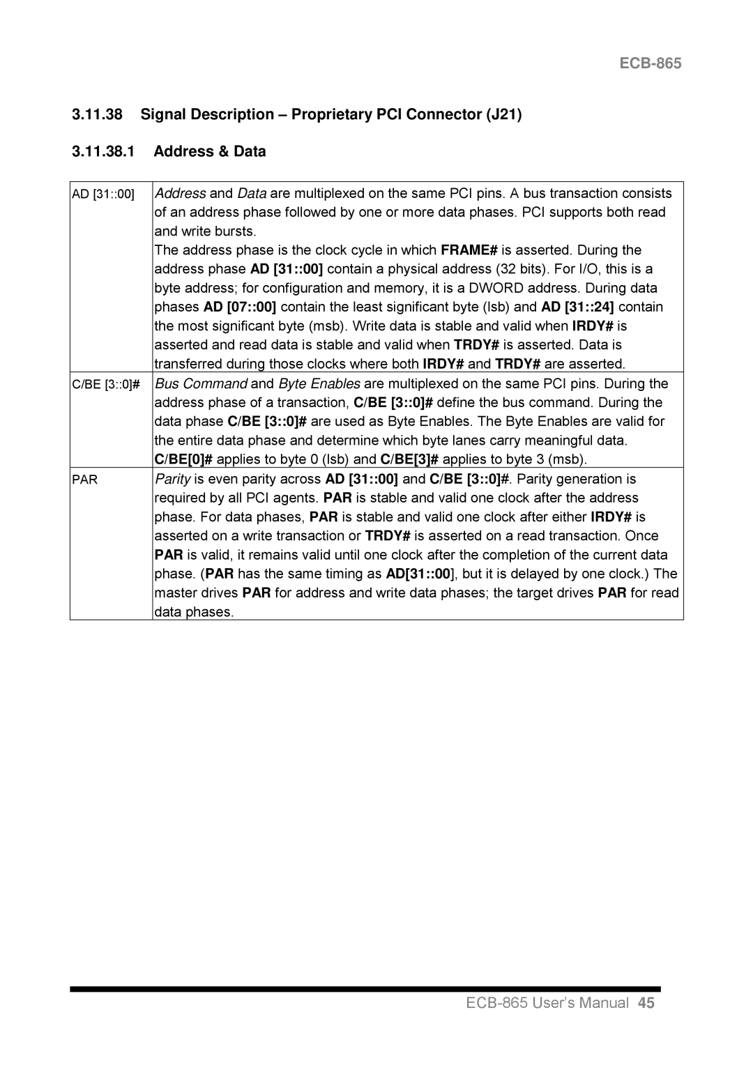
Proprietary PCI Connector J21
Write bursts
System
Interface Control
Arbitration
Error Reporting
Interrupts
Press F1 to Run Setup or Resume
AMI Bios Setup
Enter key to accept or enter the sub-menu
AMI Bios Setup Main Menu
Floppy A, Floppy B
Cmos Setup Reference Table
Standard Cmos Setup Menu
Date and Time Configuration
Master Disk, Slave Disk
Boot Sector Virus Protection
Quick Boot
Advanced Cmos Setup Defaults
Password Check
2.2 1st / 2nd / 3rd Boot Device
Try Other Boot Device
BootUp Num-Lock
System Bios Cacheable
Boot To OS/2
Shadow Memory from Address C000~DFFF, 16K Per Segment
ICH Delayed Transaction
Advanced Chipset Setup Defaults
CPU Ratio Selection
Dram Cycle time SCLKs
Sdram RAS# to CAS# Delay
Internal Graphic Mode Select
Memory Hole
Acpi Aware O/S
Power Management Setup Defaults
Power Management/ APM
Green PC Monitor Power State
Throttle Slow Clock Ratio
CPU Critical Temperature
Stand by Time Out Minute
Suspend Time Out Minute
Wake Up on Ring
Power Button Function
Wake Up on LAN
Plug and Play Aware O/S
PCI / Plug and Play Setup Defaults
Allocate IRQ to PCI VGA
PCI Latency Timer PCI Clocks
Clear Nvram
PCI / VGA Palette Snoop
OnBoard Serial Port2
Peripheral Setup Defaults
OnBoard FDC
OnBoard Serial Port1
378h
Disabled
Parallel Port Mode
On Board Parallel Port
Parallel Port DMA Channel
Parallel Port IRQ
On-Chip IDE
Hardware Monitor Setup Defaults
User’s Manual
Driver Installation for Ethernet Adapter Windows
Driver Installation
User’s Manual
ECB-865
User’s Manual
ECB-865
Windows NT 4.0 Ethernet Installation
ECB-865
User’s Manual
ECB-865
User’s Manual
Driver Installation for Display Adapter Windows
User’s Manual
ECB-865
User’s Manual
ECB-865
Windows NT 4.0 Display Installation
ECB-865
User’s Manual
ECB-865
Measurement Drawing
Bios Rev New Features Bugs/Problems Solved Known Problems
Appendix a Bios Revisions
Memory Map
Appendix B System Resources
Port Description
Map
User’s Manual
Interrupt Description
Interrupt Usage
DMA-channel Description
DMA-channel Usage
If it beeps… Then…
Appendix C Amibios Power-On Self Test
Code Description
Appendix D Amibios Post Check Point List
Bios
User’s Manual
Present
User’s Manual
ECB-865
User’s Manual
