KX-P7105 KX-P7110
KX-P7105 / KX-P7110
Contents
KX-P7105 / KX-P7110
Printer
Specifications
Paper
Interface, Options, Accessories, and Supplies
Others About Media
Margins and Print Area
Printer Panel Indicators
Indicators
Print / Reset Button
Front Side View Rear Side View
Parts Identification
Component Layout and Paper Path
Electrical Components and Sensor Boards
Switches and Solenoids
Exposure
Development / Cleaning
Print Process
Charge
Transfer
Fusing
Media Tray
Paper Feed
Laser Beam
Laser Scan Unit Exposure
Operation Theory
Lens
Collimator Lens
Polygon Scanner
Cylindrical Lens and Lens
Fuser Unit
Normal Printing Mode Not Duplex Mode
Paper Ejection and Paper Switchback
Setup
Installation Requirements
KX-P7105 / KX-P7110
Installing the Upgrade Kit for PostScript or RAM Board
Material Required
Repacking
KX-P7105 / KX-P7110
KX-P7105 / KX-P7110
Front and Rear Covers
Removal and Replacement Procedures
Rear Cover Disassembly
Front Cover Disassembly
Top Cover
Right, Left and Top Covers
Right Cover
Left Cover
Relay Board B
Laser Scanning Unit LSU
High Voltage Board
High Voltage Board and Power Supply Unit
Power Supply Unit Disassembly
Power Supply Unit
Engine Control Board
Indicator Board
Engine Control Board and Toner Empty Sensor Board
Toner Empty Sensor Board
Nd Feeder I / F Board and Main Control Board
Nd Feeder I / F Board and Main Control Board
Fan Motor
Main Control Board Disassembly
Fuser Drive Gear
Relay Board a , Drive Gear Unit and Motor
Gear Support Bracket
Paper Empty Sensor Board
Drive Gear Unit Disassembly
Upper Exit Roller Holder
Upper Exit Roller Holder Disassembly
Upper Exit Roller Holder
Fuser Unit Disassembly
Heat Roller
Heat Lamp
Thermostat
KX-P7105 / KX-P7110
Pickup Roller and Pickup Solenoid
Pickup, Paper Feed, Registration and Transfer Rollers
Registration Roller
Paper Feed Roller / Registration Roller
Transfer Roller Assembly
Auto Duplex Pinch and Registration Rollers
Auto Duplex Unit ADU
Auto Duplex Disassembly
KX-P7105 / KX-P7110
KX-P7105 / KX-P7110
Paper Empty Sensor Lever
Main Control Board Block Diagram
Block Diagram
Fuser Unit
Engine Control Block Diagram
Connection Diagram
Connection Diagram
Power Supply
Asic KME
Engine Control Board
Clock Circuit
Reset Circuit
Main Motor Drive Circuit
Motor Current will be cut off in case of OFF condition above
Laser Scanning Unit Control Circuit
Fuser Temperature Control Circuit
High Voltage Control Circuit
Eeprom Control Circuit
Safety Interlock SW
Registration Solenoid Driver Circuit
Solenoids Control Circuit
Pickup Control Solenoid Drive Circuit
Switchback Solenoid Drive Control Circuit
Top Sensor Circuit
Sensors Circuit
Registration Sensor Circuit
Paper Empty Sensor Circuit
Exit Sensor Circuit
Fan Control Circuit
Toner Empty Sensor Circuit
Nd Feeder I / F Circuit
2nd Feeder control signals are explained as follows
KX-P7105 / KX-P7110
Data Flow
Main Control Board
Power Supply
Clock Circuit
CPU Asic IC1 overview
CPU
Sdras
Sdram I/F
FRCS1
ROM I/F
Eepdata
SXD
Internal Engine I/F Main Board Engine Board
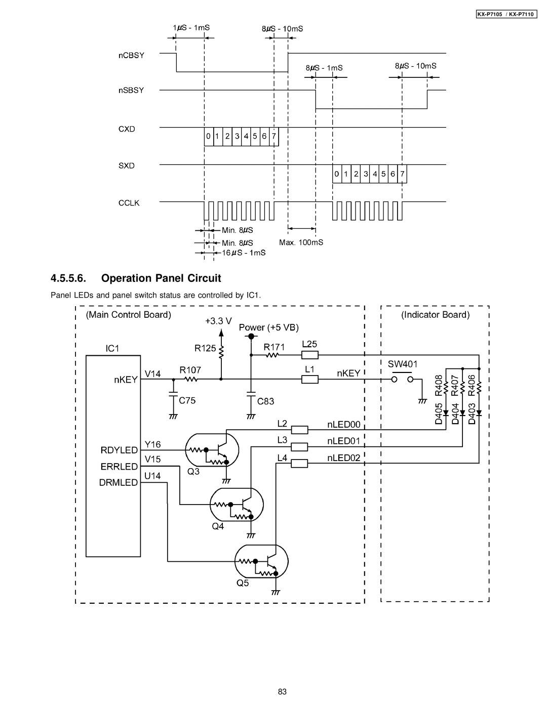
Operation Panel Circuit
Parallel I/F
USB I/F
Pcitrdy
PCI I/F
TPRDM, Tprdp
Network I/F only for KX-P7110
KX-P7105 / KX-P7110
Main Control Board
Option ROM CN
Option RAM CN
Main Control Board 4/9
IEEE1284 Circuit Block
Main Control Board 6/9
ICE Connector
Power Regulator Circuit
Main Control Board
KX-P7105 / KX-P7110
Engine Control Board
Engine Control Board 2/3
Parts Side
102
Sensors, Indicator and Relay Boards
104
Paper Empty Sensor Board, 2nd Feeder I/F Board
106
1. CN1 Optional PostScript Upgrade Kit I / F Connector
Explanation of Connectors
2. CN2 Optional RAM Connector
CN2 Optional RAM Connector
CN2
3. CN3 Network Connector
4. CN4 Ieee 1284 I / F Connector
CN4 Ieee 1284 I/F Connector
6. CN6 Front Panel Connector
5. CN5 Engine I / F Connector
1. CN001 Video Interface
7. CN9 USB I / F Connector
4. CN004 2nd Feeder
2. CN002 LSU Control Signals
3. CN003 OPC Drum Unit Interlock SW
7. CN007 Thermistor
5. CN005 PSU-MAIN Connector
8. CN008 HVU-MAIN Connector
6. CN006 Door + 24V Interlock SW
CN011 Pickup Solenoid
CN013 Switchback Solenoid
9. CN009 Toner Empty Sensor
CN010 Polygon Motor
CN018 FAN Control
14. CN014 REG-TOP Sensor
CN015 Exit Sensor
CN017 Main Motor
Paper Exit / ADU Paper Jam Sensor Board
Registration & Paper Top Sensor Board
1. CN450 Paper Empty Sensor
Paper Empty Sensor Board
Toner Empty Sensor Board
1. CN407 Fuser GND
2. CN453 to 2nd Feeder
Nd Feeder I / F Board
1. CN452 to Engine Control Board CN004
1. IC1 Main Control CPU
Component Reference Guide
IC1
GND12
2. IC2 Reset IC
4. IC5 RAM
3. IC3 Flash / Mask ROM
IC6 LAN IC
5. IC6 LAN IC
7. IC10 Regulator
6. IC7 Eeprom
8. IC12 Regulator
1. IC001 Asic
2. IC002 Comparators
3. IC003 Reset IC
5. IC005 Eeprom
4. IC004 Engine Control CPU
7. IC007 Inverters
6. IC006 Motor Drive IC
Recommended Tools
Recommended Cleaning
General
User Maintenance
Maintenance Tables
Recommended Lubrication
Service Maintenance Maintenance Cycle
Counter Reset
Lubrication
Printer Status Paper Jam
Self-Diagnostic Indicators
User Error
Call for Service
Initial Troubleshooting Flowchart
No Operation
White Vertical Line in Print
Print Quality
Blank Print
Dark Vertical Line in Print
Dark Horizontal Line in Print
Dirty Background
All-black Print
Light Print
Ghosting
Black or White Dots
Toner Spatter
Jam at a
Paper Jam
Jam at B
Jam at C
Jam at D, E
Jam at STD
Jam at OP
1. E20
Call Service
156
2. E30
3. E31
4. E32
5. E50
6. E54 7. E71
8. E73
9. E81
10. E90
11. E91
12. E96
Exterior
Replacement Parts List with Lubrication Guide
168
169
Right Side Parts
170
Engine Control Board Connector
Pickup Roller and Paper Feed Roller
Motor and Drive Gear Unit
Left Side Parts Power Supply Unit and High Voltage Board
Rear and Top Side Parts
176
Fuser Unit
177
178
Bottom Side Parts
179
Mechanical Base
Media Tray Paper Cassette
Packing
Component Side View
Parts Side View
Resistors
ICs
Capacitors
Transistor and Diodes
10.9.6 Others
10.9.5 Connectors
188
189
190
191
Resistor values is in OHMs
Registration & Paper Top Detection Sensor Board
Resistor values are in OHMs
Relay Board a
194