Alignments | DVD963SA |
| 8. |
| EN 77 |
8. Alignments
Not applicable.
9. Circuit Descriptions and List of Abbreviations
Index of this chapter:
9.2.3Operation
1.Introduction
2.Power Supply Unit (PSU).
3.Loader/Mono Board.
4.Audio Video (A/V) Board.
5.Front Display Board.
6.Abbreviations
7.IC Data
Notes:
•See also the SD4.00SA_CH Service Manual (3122 785 12480).
•Figures can deviate slightly from the actual situation, due to different set executions.
•For a good understanding of the following circuit descriptions, please use the diagrams in chapter 6 and 7. Where necessary, you will find a separate drawing for clarification.
9.1Introduction
The DVD963SA is a model from the SACD 2002 'single disc' range. It uses a 2nd generation Philips SACD mono board, based on the Furore 2 DSD/DST decoder.
MAINS ![]()
![]() DM1
DM1
CM1
RECTIFIER |
|
AC | 300V |
| C5 |
DC |
|
| Q1 |
IC1 | D |
112 ![]() G
G![]()
![]()
![]()
![]()
S
5 11
4 13
RSENSE1
![]() C7
C7
T1
![]() +12V
+12V
etc
![]() +12V
+12V
IC2
![]() IC3
IC3
RSENSE2
CL 26532053_024.eps 010502
Below you will find a circuit description of the several modules.
9.2Power Supply Unit
9.2.1Introduction
This supply is a Switching Mode Power Supply (SMPS), which uses the control IC TY720xx to produce pulses to drive the power ‘switch’ (MOSFET). The TY720xx (IC7130) is a high performance, current mode controller for
The operation frequency varies with the circuit load. When the output power demand decreases, the switching frequency raises, with a maximum frequency of 125 kHz (defined by C2130 at pin 5). At this point, the internal VCO takes over and starts to decrease the switching frequency.
This has some benefits compared to a ‘fixed frequency’ flyback converter. The efficiency is better, which results in a lower power consumption.
9.2.2Output Voltages
The following output voltages are present on connector 0201:
•Pin 1 and 2: +3V3.
•Pin 4: +12V
•Pin 5: +12STBY.
•Pin 7: +5V.
•Pin 9:
•Pin 11:
Note: The suffix 'STBY' indicates that the supply is not switched 'off' during Standby Mode. Power switching is done with the STBY_CTRL signal from the slave processor.
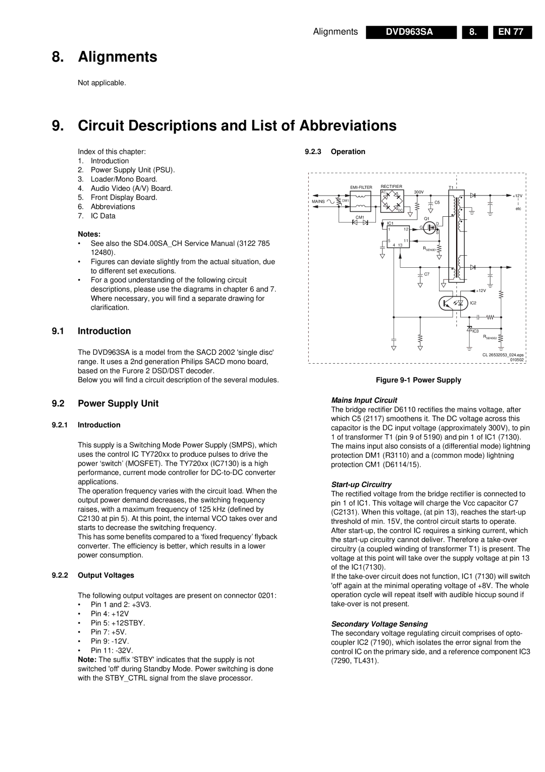
Figure 9-1 Power Supply
Mains Input Circuit
The bridge rectifier D6110 rectifies the mains voltage, after which C5 (2117) smoothens it. The DC voltage across this capacitor is the DC input voltage (approximately 300V), to pin 1 of transformer T1 (pin 9 of 5190) and pin 1 of IC1 (7130). The mains input also consists of a (differential mode) lightning protection DM1 (R3110) and a (common mode) lightning protection CM1 (D6114/15).
Start-up Circuitry
The rectified voltage from the bridge rectifier is connected to pin 1 of IC1. This voltage will charge the Vcc capacitor C7 (C2131). When this voltage, (at pin 13), reaches the
If the
Secondary Voltage Sensing
The secondary voltage regulating circuit comprises of opto- coupler IC2 (7190), which isolates the error signal from the control IC on the primary side, and a reference component IC3 (7290, TL431).