Circuit Descriptions and List of Abbreviations | DVD963SA |
| 9. |
| EN 83 |
The SACD DSD/DST decoder Furore 2 uses 1.8V for its core and analogue portion, and 3.3V for its interface. The
The
Reset Circuit
9.4.2Control
The control of the A/V board is done by
Table 9-2 Control lines overview IC7107
Description | Pin | Hi | Lo |
CLK_SEL | 12 | External clock | Internal clock |
|
| (DSD stream) | (PCM stream) |
|
|
|
|
UPSAMPLING | 11 | No upsampling | Upsampling |
|
|
|
|
DAC_RESET | 10 | Normal | Reset |
|
|
|
|
CENTER_ON | 9 | Off | On |
|
|
|
|
| 5 | Mute | No mute |
Low Voltage Detection 4.5V
STi55xx
Power On |
| |
Reset | RESETn | |
Circuit | ||
| ||
Delay 1 |
|
Furore 2
192k/96k | 4 192k PCM | 96k PCM |
9.4.3 Video |
The analogue video signals from the Mono Board are buffered |
before they are fed to the A/V board. The video outputs from |
the A/V Board are RGB/YUV, YC, and CVBS. These signals |
Low Voltage Detection 4.5V
RSTN![]()
Power On
Reset
Circuit
Delay ![]() 2
2
CLK_STBCTRL
Clock Factory
RES_P | Basic Engine |
|
CL 26532053_018.eps 260402
are also fed to the double SCART board. |
9.4.4 Audio |
The digital audio signals for Surround, Centre and LFE |
(subwoofer) are fed to a |
and PCM data streams. |
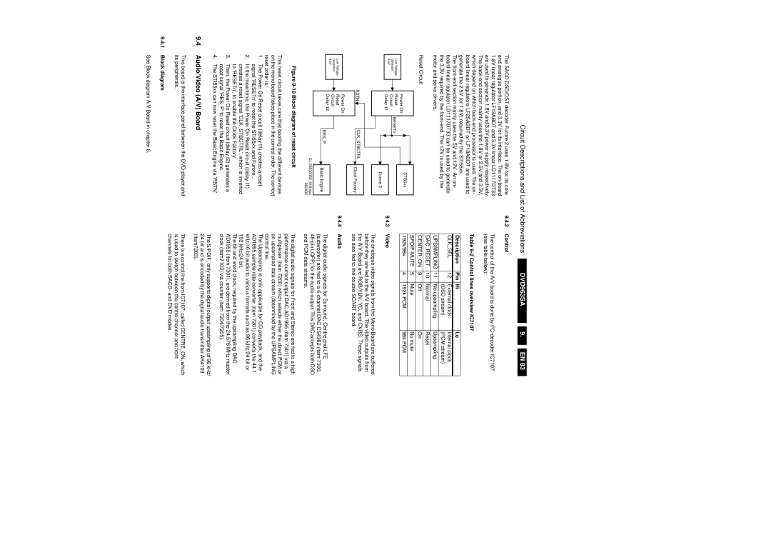
Figure 9-10 Block diagram of reset circuit
This reset circuit takes care that booting the different devices on the mono board takes place in the correct order. The correct reset order is:
1.The Power On Reset circuit (delay t1) creates a reset signal 'RESETn' to reset the STi55xx and Furore .
2.In the meantime, the Power On Reset circuit (delay t1) creates a reset signal 'CLK_STBCTRL', which is inverted to 'RESETn', to enable the Clock Factory.
3.Then, the Power On Reset circuit (delay t2) generates a reset signal 'RES_P' to reset the Basic Engine.
4.The STI55xx can now reset the Basic Engine via 'RSTN'.
9.4Audio/Video (A/V) Board
This board is the interface panel between the
9.4.1Block diagram
The digital audio signals for Front and Stereo are fed to a high |
performance current output DAC AD1955 (item 7301) via a |
multiplexer (item 7200) which selects either the direct PCM or |
an upsampled data stream (determined by the UPSAMPLING |
control line. |
The Upsampling is only applicable for CD playback, and the |
AD1895 sample rate converter (item 7201) converts the 44.1 |
kHz/16 bit audio to various formats such as 96 kHz/24 bit or |
192 kHz/24 bit. |
The bit and word clock, required by the upsampling DAC |
AD1955 (item 7301), are derived from the 24.576 MHz master |
clock (item7103) via counter (item 7204/7205). |
The S/PDIF, only supports digital output upsampling of 96 kHz/ |
24 bit and is encoded by the digital audio transmitter AK4103 |
(item7203). |
There is a control line from IC7107, called CENTRE_ON, which |
is used to switch between the centre channel and front |
channels for both SACD- and DVD modes. |
See Block diagram A/V Board in chapter 6.
