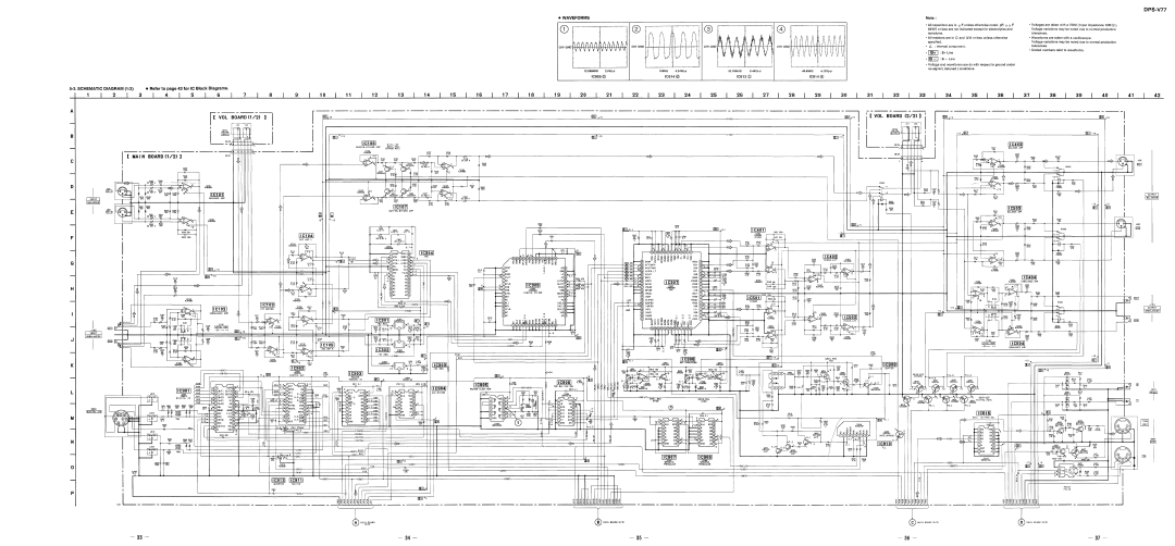
• WAVEFORMS
CD
IP.288MHz | IOMHz | 32.768kHz | 48.6MHz | 4,/2Vp_p | |
IC905<!j) | IC614@ | IC613 <Z) | IC914@ | ||
Note:
•All capacitors are in ~ F unless otherwise noted. pF: I.J. 1.1 F 50WV or less are not indicated except for electrolytics and tantalums.
•All resistors are in Q and Y4W or less unless otherwise specified.
•1::. : internal component.
·rn±J ;B+ Line
•IB - I : B - line
•Voltage and waveforms are de with respect to ground under
DPS-V77
•Voltages are taken with a YOM (Input impedance 10M Q).
Voltage variations may be noted due to normal production tolerances.
•Waveforms are taken with a oscillo$l;:ope.
Voltage variations may be noted due to normal production tolerances.
•Circled numbers refer to waveforms.
1 | 2 | 345 | 6 | 7 | 8 | 9 | 10 | 11 | 12 | 13 | 14 | 15 | 16 | 17 | 18 | 19 | 20 | 21 | 22 | 23 | 25 | 26 | 27 | 28 | 29 | 30 | 31 | 32 | 33 | 34 | 35 | 36 |
A
B
c
o
E
F
G
H
__1..!.2.L......
INPUT
UNBALANCEil .
J
I(I
I
I
L | I | 19l~ | 1leB011 |
| |||
|
| ||
~r;s~1 |
|
|
|
1!i15lTAL | 170' |
|
|
M |
| l.~.j ~.Ol | "" |
|
| ||
N
o
p
'"
3738 39404142
OUTPUT
BALANCEil
I
j I 04
OUTPUT
UNBIoLl<NCEil
I
J~O I
IillIiJ,
nRul
lOUT
- 33- | - 34- | - 35- | - 36- | - 37- |