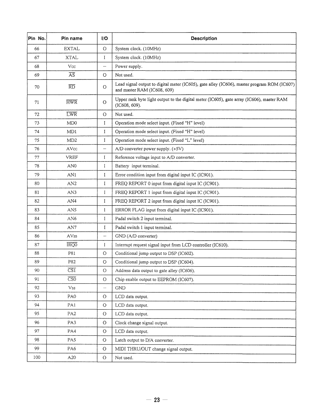
Pin No. |
| Pin name |
| I/O |
| Description | ||||||
|
|
|
|
|
|
|
|
|
|
|
|
|
66 |
|
| EXTAL | 0 |
| System clock. (lOMHz) | ||||||
|
|
|
|
|
|
|
|
|
|
|
|
|
67 |
|
| XTAL |
| I |
| System clock. (lOMHz) | |||||
|
|
|
|
|
|
|
|
|
|
|
|
|
68 |
|
| Vee | - |
| Power supply. | ||||||
|
|
|
|
|
|
|
|
|
|
|
|
|
69 |
|
| AS | 0 |
| Not used. | ||||||
|
|
|
|
|
|
|
|
|
|
|
|
|
70 |
|
| RD | 0 |
| Lead signal output to digital meter (lC605), gate alley (lC606), master program ROM (lC607) | ||||||
|
|
| and master RAM (lC608, 609) | |||||||||
|
|
|
|
|
|
| ||||||
|
|
|
|
|
|
|
|
|
|
|
|
|
71 |
|
| HWR | 0 |
| Upper rank byte light output to the digital meter (IC605), gate array (IC606), master RAM | ||||||
|
|
| (lC608,609). | |||||||||
|
|
|
|
|
|
| ||||||
|
|
|
|
|
|
|
|
|
|
|
|
|
72 |
|
| LWR | 0 |
| Not used. | ||||||
|
|
|
|
|
|
|
|
|
|
|
|
|
73 |
|
| MDO |
| I |
| Operation mode select input. (Fixed "H" level) | |||||
|
|
|
|
|
|
|
|
|
|
|
|
|
74 |
|
| MDI |
| I |
| Operation mode select input. (Fixed "H" level) | |||||
|
|
|
|
|
|
|
|
|
|
|
|
|
75 |
|
| MD2 |
| I |
| Operation mode select input. (Fixed "L" level) | |||||
|
|
|
|
|
|
|
|
|
|
|
|
|
76 |
|
| AVee | - |
| AID converter power supply. (+5V) | ||||||
|
|
|
|
|
|
|
|
|
|
|
|
|
77 |
|
| VREF |
| I |
| Reference voltage input to AID converter. | |||||
|
|
|
|
|
|
|
|
|
|
|
|
|
78 |
|
| ANO |
| I |
| Battery input terminal. | |||||
|
|
|
|
|
|
|
|
|
|
|
|
|
79 |
|
| ANI |
| I |
| Error condition input from digital input IC (IC90l). | |||||
|
|
|
|
|
|
|
|
|
|
|
|
|
80 |
|
| AN2 |
| I |
| FREQ REPORT 0 input from digital input IC (IC90l). | |||||
|
|
|
|
|
|
|
|
|
|
|
|
|
81 |
|
| AN3 |
| I |
| FREQ REPORT 1 input from digital input IC (lC90l). | |||||
|
|
|
|
|
|
|
|
|
|
|
|
|
82 |
|
| AN4 |
| I |
| FREQ REPORT 2 input from digital input IC (lC90l). | |||||
|
|
|
|
|
|
|
|
|
|
|
|
|
83 |
|
| AN5 |
| I |
| ERROR FLAG input from digital input IC (lC90l). | |||||
|
|
|
|
|
|
|
|
|
|
|
|
|
84 |
|
| AN6 |
| I |
| Padal switch 2 input terminal. | |||||
|
|
|
|
|
|
|
|
|
|
|
|
|
85 |
|
| AN7 |
| I |
| Padal switch 1 input terminal. | |||||
|
|
|
|
|
|
|
|
|
|
|
|
|
86 |
|
| AVss | - |
| GND (AID converter) | ||||||
|
|
|
|
|
|
|
|
|
|
|
|
|
87 |
|
| IRQO |
| I |
| Interrupt request signal input from LCD controller (lC6l0). | |||||
|
|
|
|
|
|
|
|
|
|
|
|
|
88 |
|
| P8I | 0 |
| Conditional jump output to DSP (lC602). | ||||||
|
|
|
|
|
|
|
|
|
|
|
|
|
89 |
|
| P82 | 0 |
| Conditional jump output to DSP (lC604). | ||||||
|
|
|
|
|
|
|
|
|
|
|
|
|
90 |
|
| CSI | 0 |
| Address data output to gate alley (lC606). | ||||||
|
|
|
|
|
|
|
|
|
|
|
|
|
91 |
|
| CSO | 0 |
| Chip enable output to EEPROM (lC607). | ||||||
|
|
|
|
|
|
|
|
|
|
|
|
|
92 |
|
| Vss | - |
| GND | ||||||
|
|
|
|
|
|
|
|
|
|
|
|
|
93 |
|
| PAO | 0 |
| LCD data output. | ||||||
|
|
|
|
|
|
|
|
|
|
|
|
|
94 |
|
| PAl | 0 |
| LCD data output. | ||||||
|
|
|
|
|
|
|
|
|
|
|
| |
95 |
|
| PA2 | 0 |
| LCD data output. | ||||||
|
|
|
|
|
|
|
|
|
|
|
| |
96 |
|
| PA3 | 0 |
| Clock change signal output. | ||||||
|
|
|
|
|
|
|
|
|
|
| ||
97 |
|
| PA4 | 0 |
| LCD data output. | ||||||
|
|
|
|
|
|
|
|
|
| |||
98 |
|
| PAS | 0 |
| Latch output to 0/A converter. | ||||||
|
|
|
|
|
|
|
|
| ||||
99 |
|
| PA6 | 0 |
| MIDI THRU/OUT change signal output. | ||||||
|
|
|
|
|
|
|
|
| ||||
100 |
|
| A20 | 0 |
| Not used. | ||||||
|
|
|
|
|
|
|
|
|
|
|
|
|
|
|
|
|
|
|
|
|
|
|
|
|
|
- 23-