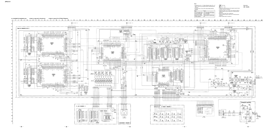
DPS-V77
5·4.SCHEMATIC DIAGRAM (2/2)
Note:
•All capacitors are in 1.1 F unless otherwise noted. pF: !J !J F 50WV or less are not indicated except for electrolytics and tantalulTls.
•All resistors are in Q and WW or less unless otherwise speCified.
Note:Note:
The components identi- Les composa~ts identifies par | |
fied by mark Lh arda!- | une marque ffi sont critiques |
ted line with mark ,& | pour la securite. |
are critical for safety. | Ne les rempJacer que par une |
Replace only with part | piece portant Ie numero sped- |
number specified, | fie, |
·rn±J :B+ LIne
· EJ:8 - Line
•Voltage and waveforms are de with respect to ground under
•Voltages are taken with a YOM (Input impedance 10M Q). Voltage variations may be noted due to normal production tolerances.
•Waveforms are taken with a oscilloscope.
Voltage variations may be noted due to normal production tolerances.
•Circled numbers reler to waveforms.
•Abbreviation eND: Canadian AUS . Australian
123
43
A
B
c | "" | "" |
Wr | 0.1 | |
|
|
D
E
F
G
H
. em ,.
, ,
§!
1 E..29 '"
Efl~ .. ;'
.,
J
K
L
u
N
a
p
Q
R
c~ MAlN ~UAR~ (1/2)
*'1.'1
em
LROF
~ ,", ..,
,.
~MA [N EUAHB fl/21
|
|
| |
|
| IE] | , |
"Iii .~ ~
(~:~, |
| , , | |
" | ". | ||
|
A6 AS
A5 r;.l ~9
~:
AO !ll
BI g
! | __ 'ISS |
Ilcsosl
II I | I | I | I | I | I |
""
"" . | , , | " , | , , |
'i; |
|
|
|
* ~ | WOO | " | ' < |
"~ | •• 31 | ||
,., | 1'1.'1 |
|
|
"'" |
|
|
|
, | II vee | IICS10I |
|
" | ,aihWFOOl |
| |
| , " |
| |
|
|
| |
| , " |
|
|
| ',M |
|
|
..~ | " |
|
|
" |
|
| |
| Xfl3 |
|
|
| ~ "', |
|
|
| , |
|
|
(10~EY B;ARD 1
-- I
I | |
| I |
| I |
| I |
| I |
~ MAIN BUARIJ 11/21 | ~ MAIN 30ARO <1/21 |
1111
|
| 1 |
|
|
| ! |
|
i | i | 'I'lf:'~1~1'rr~·'· |
|
i |
|
| |
I |
|
|
|
I |
| I |
|
I |
|
| |
|
|
| |
I |
| i LC{l | |
i |
|
|
|
I
I
I
LCESOl
LeE MOflULE
IFBOI - F"ao~
[T.I'}[~iYJ ~Er. ~us
I
I
I
I
I
~J
- 38- | - 39- | - 40- | - 41 | - 42- |