TT Base Assy
Specifications
OPTIMA-720L1E
MDM-7B4M
SELF-DIAGNOSIS Function
HCD-C5
Electrical Adjustments
Table of Contents
Diagrams
Exploded Views Electrical Parts List
HCD-C5 Section Servicing Note
Flexible Circuit Board Repairing
Service Position of the MD Mechanism Deck
Service Position of the CD Mechanism Deck
IOP
JIG for Checking BD MD Board Waveform
Parts Identification
Section General
Parts Identification
Remote control
SET Bottom PLATE, Case
HCD-C5 Section Disassembly
Panel Board
Bottom PLATE, Case
CN1
CD Mechanism Deck TN-CCD1001Z, BD CD Board
Connector Board
Front Bracket SECTION, Loading Motor Assy M902
SW Board
Rear Damper Bracket
Feed Motor Assy M903
Optical PICK-UP OPTIMA-720L1E
Base Section
Jack BOARD, HP BOARD, Rear Cover
Spindle Motor Assy M904
Tuner PACK, D. C. FAN M901
Ucom BOARD, AMP Power Board
Connector CN105
Audio BOARD, Power BOARD, Power Transformer T900
Holder Assy
MD Mechanism Deck MDM-7B4M, MD Digital Board
Loading Motor M703, Spindle Motor M701, Sled Motor M702
BD MD Board
OP-SUB Section
Over Write Head
HCD-C5 Section Test Mode
Setting the Test Mode
Precautions for USE of Test Mode
Releasing the Test Mode
MD Seciton
Basic Operations of the Test Mode
Selecting the Test Mode
ENTER/YES R
Operating the Continuous Playback Mode
Functions of Other Buttons
Automatic SELF-DIAGNOSIS Function
Information
When Memory NG is Displayed
Record Procedure
Display Precedure
Retry Cause Display Mode in MD
Checks Prior to Parts Replacement and Adjustments in MD
Criteria for Determination Measure if unsatisfactory
Precedure
Reading the Retry Cause Display
Reading the Display
Example
Details
Bit When Binary
Section Electrical Adjustments HCD-C5
CD Section
RF Level Check
Parts Replacement and Adjustment
Check before replacement
MD Section
YES
Adjustment flow
Precautions for USE of Optical PICK-UP KMS-260B/260E
Precautions for Checking Laser Diode Emission
Precautions for Adjustments
Laser power meter
Temperature Compensation Offset Check
Using the Continuously Recorded Disc
Laser Power Check
Checks Prior to Repairs
Auto Check
Other Checks
Traverse Check
Focus Bias Check
Play Check
Self-Recording/playback Check
Temperature Compensation Offset Adjustment
Initial Setting of Adjustment Value
Laser Power Adjustment
Recording and Displaying the IOP Information
Traverse Adjustment
Method of identifying the optical pick-up KMS-260B/260E
Iop NV Save
Read power traverse adjustment
Error Rate Check
Focus Bias Adjustment
CD Error Rate Check
MO Error Rate Check
CD Auto Gain Control Output Level Adjustment
Auto Gain Control Output Level Adjustment
MO Auto Gain Control Output Level Adjustment
Adjustment and checking Loacation
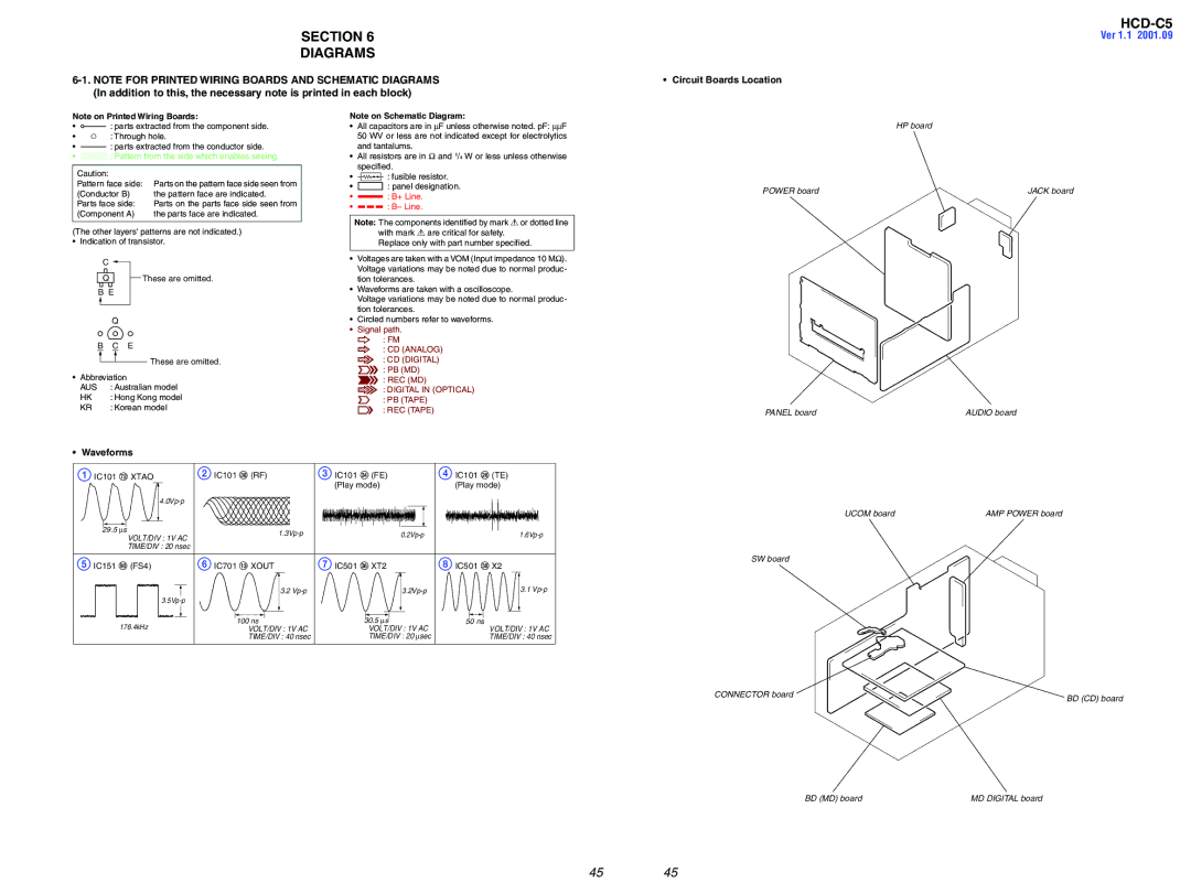
Circuit Boards Location
Section Diagrams HCD-C5
Waveforms
AUS
OPTIMA-720L1E
Block Diagram CD Servo Section
APC
Block Diagram MD Servo Section
Tape MD-L
Block Diagram Main Section
Semiconductor
Location
IC B/D
Location Side B
Location Side a
IC B/D
153
IC201
10K 1/16W
Semiconductor Location
Printed Wiring Board Ucom Board
Digital Optical Input Speaker
IC302
D301 1SS355TE
IC602
HCD-C5
IC901
Schematic Diagram Power Section
IC Block Diagrams
IC101 CXD3068Q BD CD Board IC103 CXA2581N-T4 BD CD Board
IC102 BA5982FP-E2 BD CD Board
IC141 BH6519FS-E2 BD MD Board
IC201 ∝ DA1360TS MD Digital Board
Rtcb Vddd PREEM0 NC NC TEST2
Selstatic TEST1 Reset Bcko Vddd C
Vssd
Vssd C L3DATA
IC601 M66004M8FP-200D Panel Board
IC101
IC PIN Function Description
Sens
Srdt
Xrst
Sqsy
Asyi
Asyo
Avdd
Bias
Spfd
TEST1
TEST2 TEST3 Dvss
IC701
DA-RESET
Reset
PLAY-SW
REC-SW
IC501
Help
SPK-RELAY
Bvdd
Bvss
Overall Section
Section Exploded Views
Front Panel Section
102 104 111 103 112 114 105 101 106 107 108
Chassis
110
113
156 157 151 158
155 154
152
155 A-4725-732-A MD Digital BOARD, Complete
CD Mechanism Deck Section TN-CCD1001Z
CD Mechanism Deck Secti Front Bracket Section TN-CCD1001Z
CD Mechanism Deck Section Base Section TN-CCD1001Z
CD Mechanism Deck Section Chassis Section TN-CCD1001Z
MD Mechanism Deck MDM-7B4M
760 762 763 764 759
761
758 761 757 756 751
753754 755 752
AMP Audio Section Electrical Parts List
BD CD
Audio HCD-C5
HCD-C5 BD CD
CONNECTOR, FFC 29P
Diode UDZ-TE-17-3.9B Ferrite Bead
Ferrite
BD CD HCD-C5 BD MD
HCD-C5 BD MD
MD Digital
BD MD Connector Jack HCD-C5
Ferrite Bead / Conductor
HCD-C5 MD Digital Panel
Ferrite 0UH
Inductor
Panel Power
Power Ucom
CONNECTOR, Round Type 6P
CONNECTOR, FFC 16P
Connector DIN 8P
PIN, Connector 4P Diode
R225 216-841-11
Switch Detection Limit
Wire Flat Type 19 Core
TRANSFORMER, Power AEP,UK,AUS
Hardware List
HCD-C5 Revision History