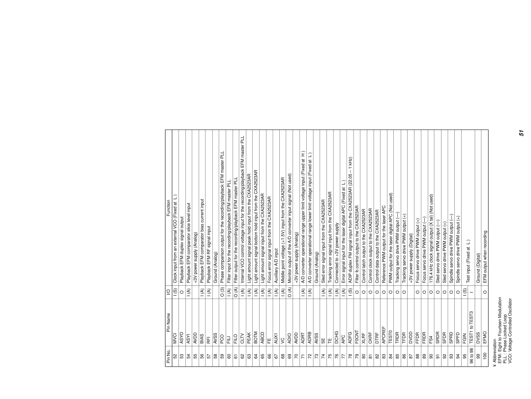
Pin No. | Pin Name | I/O | Function | |
|
|
|
| |
52 | MVCI | I (S) | Clock input from an external VCO (Fixed at “L”) | |
|
|
|
| |
53 | ASYO | O | Playback EFM duplex signal output | |
|
|
|
| |
54 | ASYI | I (A) | Playback EFM comparator slice level input | |
|
|
|
| |
55 | AVDD | — | +3V power supply (Analog) | |
|
|
|
| |
56 | BIAS | I (A) | Playback EFM comparator bias current input | |
|
|
|
| |
57 | RFI | I (A) | Playback EFM RF signal input | |
|
|
|
| |
58 | AVSS | — | Ground (Analog) | |
|
|
|
| |
59 | PCO | O (3) | Phase comparison output for the recording/playback EFM master PLL | |
|
|
|
| |
60 | FILI | I (A) | Filter input for the recording/playback EFM master PLL | |
|
|
|
| |
61 | FILO | O (A) | Filter output for the recording/playback EFM master PLL | |
|
|
|
| |
62 | CLTV | I (A) | Internal VCO control voltage input for the recording/playback EFM master PLL | |
|
|
|
| |
63 | PEAK | I (A) | Light amount signal peak hold input from the CXA2523AR | |
|
|
|
| |
64 | BOTM | I (A) | Light amount signal bottom hold input from the CXA2523AR | |
|
|
|
| |
65 | ABCD | I (A) | Light amount signal input from the CXA2523AR | |
|
|
|
| |
66 | FE | I (A) | Focus error signal input from the CXA2523AR | |
|
|
|
| |
67 | AUX1 | I (A) | Auxiliary A/D input | |
|
|
|
| |
68 | VC | I (A) | Middle point voltage (+1.5V) input from the CXA2523AR | |
|
|
|
| |
69 | ADIO | O (A) | Monitor output of the A/D converter input signal (Not used) | |
|
|
|
| |
70 | AVDD | — | +3V power supply (Analog) | |
|
|
|
| |
71 | ADRT | I (A) | A/D converter operational range upper limit voltage input (Fixed at “H”) | |
|
|
|
| |
72 | ADRB | I (A) | A/D converter operational range lower limit voltage input (Fixed at “L”) | |
|
|
|
| |
73 | AVSS | — | Ground (Analog) | |
|
|
|
| |
74 | SE | I (A) | Sled error signal input from the CXA2523AR | |
|
|
|
| |
75 | TE | I (A) | Tracking error signal input from the CXA2523AR | |
|
|
|
| |
76 | DCHG | I (A) | Connected to +3V power supply | |
|
|
|
| |
77 | APC | I (A) | Error signal input for the laser digital APC (Fixed at “L”) | |
|
|
|
| |
78 | ADFG | I (S) | ADIP duplex FM signal input from the CXA2523AR (22.05 ± 1 kHz) | |
|
|
|
| |
79 | F0CNT | O | Filter f0 control output to the CXA2523AR | |
|
|
|
| |
80 | XLRF | O | Control latch output to the CXA2523AR | |
|
|
|
| |
81 | CKRF | O | Control clock output to the CXA2523AR | |
|
|
|
| |
82 | DTRF | O | Control data output to the CXA2523AR | |
83 | APCREF | O | Reference PWM output for the laser APC | |
|
|
|
| |
84 | TEST0 | O | PWM output for the laser digital APC (Not used) | |
|
|
|
| |
85 | TRDR | O | Tracking servo drive PWM output | |
|
|
|
| |
86 | TFDR | O | Tracking servo drive PWM output (+) | |
|
|
|
| |
87 | DVDD | — | +3V power supply (Digital) | |
|
|
|
| |
88 | FFDR | O | Focus servo drive PWM output (+) | |
|
|
|
| |
89 | FRDR | O | Focus servo drive PWM output | |
|
|
|
| |
90 | FS4 | O | 176.4 kHz clock signal output (X’tal) (Not used) | |
|
|
|
| |
91 | SRDR | O | Sled servo drive PWM output | |
|
|
|
| |
92 | SFDR | O | Sled servo drive PWM output (+) | |
|
|
|
| |
93 | SPRD | O | Spindle servo drive PWM output | |
|
|
|
| |
94 | SPFD | O | Spindle servo drive PWM output (+) | |
|
|
|
| |
95 | FGIN | I (S) | Test input (Fixed at “L”) | |
|
|
| ||
96 to 98 | TEST1 to TEST3 | I | ||
| ||||
|
|
|
| |
99 | DVSS | — | Ground (Digital) | |
100 | EFMO | O | EFM output when recording | |
|
|
|
|
•Abbreviation
EFM: Eight to Fourteen Modulation
PLL : Phase Locked Loop
VCO: Voltage Controlled Oscillator
51