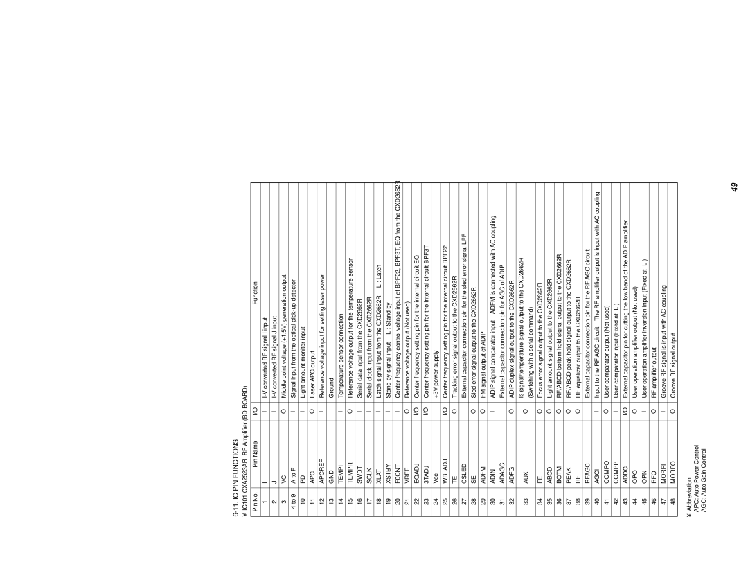
6-11. IC PIN FUNCTIONS
• IC101 CXA2523AR RF Amplifier (BD BOARD)
Pin No. | Pin Name | I/O |
| Function | |
|
|
|
| ||
1 | I | I | |||
|
|
|
| ||
2 | J | I | |||
|
|
|
| ||
3 | VC | O | Middle point voltage (+1.5V) generation output | ||
|
|
|
| ||
4 to 9 | A to F | I | Signal input from the optical | ||
|
|
|
|
| |
10 | PD | I | Light amount monitor input |
| |
|
|
|
|
| |
11 | APC | O | Laser APC output |
| |
|
|
|
| ||
12 | APCREF | I | Reference voltage input for setting laser power | ||
|
|
|
|
| |
13 | GND | — | Ground |
| |
|
|
|
| ||
14 | TEMPI | I | Temperature sensor connection | ||
|
|
|
| ||
15 | TEMPR | O | Reference voltage output for the temperature sensor | ||
|
|
|
| ||
16 | SWDT | I | Serial data input from the CXD2662R | ||
|
|
|
| ||
17 | SCLK | I | Serial clock input from the CXD2662R | ||
|
|
|
| ||
18 | XLAT | I | Latch signal input from the CXD2662R “L”: Latch | ||
|
|
|
| ||
19 | XSTBY | I | Stand by signal input “L”: Stand by | ||
|
|
|
| ||
20 | F0CNT | I | Center frequency control voltage input of BPF22, BPF3T, EQ from the CXD2662R | ||
|
|
|
| ||
21 | VREF | O | Reference voltage output (Not used) | ||
|
|
|
| ||
22 | EQADJ | I/O | Center frequency setting pin for the internal circuit EQ | ||
|
|
|
| ||
23 | 3TADJ | I/O | Center frequency setting pin for the internal circuit BPF3T | ||
|
|
|
|
| |
24 | Vcc | — | +3V power supply |
| |
|
|
|
| ||
25 | WBLADJ | I/O | Center frequency setting pin for the internal circuit BPF22 | ||
|
|
|
| ||
26 | TE | O | Tracking error signal output to the CXD2662R | ||
|
|
|
| ||
27 | CSLED | — | External capacitor connection pin for the sled error signal LPF | ||
|
|
|
| ||
28 | SE | O | Sled error signal output to the CXD2662R | ||
|
|
|
|
| |
29 | ADFM | O | FM signal output of ADIP |
| |
|
|
|
|
| |
30 | ADIN | I | ADIP signal comparator input | ADFM is connected with AC coupling | |
|
|
|
| ||
31 | ADAGC | — | External capacitor connection pin for AGC of ADIP | ||
|
|
|
| ||
32 | ADFG | O | ADIP duplex signal output to the CXD2662R | ||
|
|
|
| ||
33 | AUX | O | I3 signal/temperature signal output to the CXD2662R | ||
(Switching with a serial command) | |||||
|
|
| |||
|
|
|
| ||
34 | FE | O | Focus error signal output to the CXD2662R | ||
|
|
|
| ||
35 | ABCD | O | Light amount signal output to the CXD2662R | ||
|
|
|
| ||
36 | BOTM | O | RF/ABCD bottom hold signal output to the CXD2662R | ||
|
|
|
| ||
37 | PEAK | O | RF/ABCD peak hold signal output to the CXD2662R | ||
|
|
|
| ||
38 | RF | O | RF equalizer output to the CXD2662R | ||
|
|
|
| ||
39 | RFAGC | — | External capacitor connection pin for the RF AGC circuit | ||
|
|
|
|
| |
40 | AGCI | I | Input to the RF AGC circuit | The RF amplifier output is input with AC coupling | |
|
|
|
| ||
41 | COMPO | O | User comparator output (Not used) | ||
|
|
|
| ||
42 | COMPP | I | User comparator input (Fixed at “L”) | ||
|
|
|
| ||
43 | ADDC | I/O | External capacitor pin for cutting the low band of the ADIP amplifier | ||
44 | OPO | O | User operation amplifier output (Not used) | ||
45 | OPN | I | User operation amplifier inversion input (Fixed at “L”) | ||
|
|
|
|
| |
46 | RFO | O | RF amplifier output |
| |
|
|
|
| ||
47 | MORFI | I | Groove RF signal is input with AC coupling | ||
|
|
|
|
| |
48 | MORFO | O | Groove RF signal output |
| |
|
|
|
|
| |
•Abbreviation
APC: Auto Power Control
AGC: Auto Gain Control
49