SECTION 6
DIAGRAMS
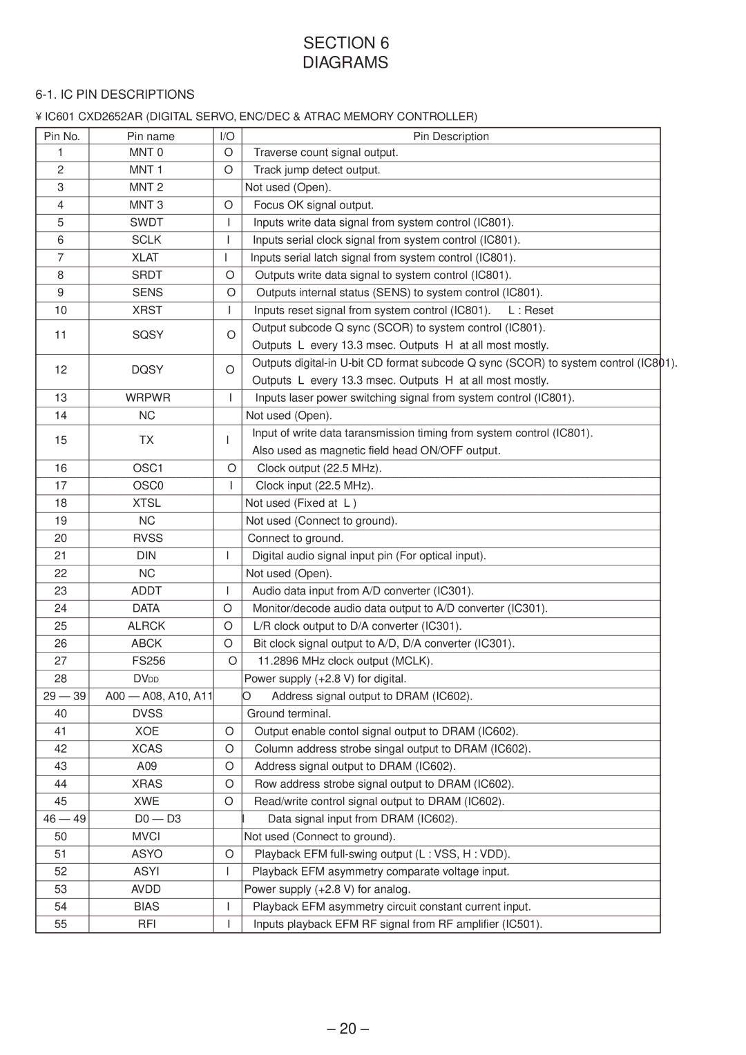
6-1. IC PIN DESCRIPTIONS
• IC601 CXD2652AR (DIGITAL SERVO, ENC/DEC & ATRAC MEMORY CONTROLLER)
Pin No. | Pin name | I/O | Pin Description | |
1 | MNT 0 | O | Traverse count signal output. | |
|
|
|
| |
2 | MNT 1 | O | Track jump detect output. | |
|
|
|
| |
3 | MNT 2 | — | Not used (Open). | |
|
|
|
| |
4 | MNT 3 | O | Focus OK signal output. | |
|
|
|
| |
5 | SWDT | I | Inputs write data signal from system control (IC801). | |
|
|
|
| |
6 | SCLK | I | Inputs serial clock signal from system control (IC801). | |
|
|
|
| |
7 | XLAT | I | Inputs serial latch signal from system control (IC801). | |
|
|
|
| |
8 | SRDT | O | Outputs write data signal to system control (IC801). | |
|
|
|
| |
9 | SENS | O | Outputs internal status (SENS) to system control (IC801). | |
|
|
|
| |
10 | XRST | I | Inputs reset signal from system control (IC801). L : Reset | |
|
|
|
| |
11 | SQSY | O | Output subcode Q sync (SCOR) to system control (IC801). | |
Outputs “L” every 13.3 msec. Outputs “H” at all most mostly. | ||||
|
|
| ||
|
|
|
| |
12 | DQSY | O | Outputs | |
Outputs “L” every 13.3 msec. Outputs “H” at all most mostly. | ||||
|
|
| ||
|
|
|
| |
13 | WRPWR | I | Inputs laser power switching signal from system control (IC801). | |
|
|
|
| |
14 | NC | — | Not used (Open). | |
|
|
|
| |
15 | TX | I | Input of write data taransmission timing from system control (IC801). | |
Also used as magnetic field head ON/OFF output. | ||||
|
|
| ||
|
|
|
| |
16 | OSC1 | O | Clock output (22.5 MHz). | |
|
|
|
| |
17 | OSC0 | I | Clock input (22.5 MHz). | |
|
|
|
| |
18 | XTSL | — | Not used (Fixed at “L”) | |
|
|
|
| |
19 | NC | — | Not used (Connect to ground). | |
|
|
|
| |
20 | RVSS | — | Connect to ground. | |
|
|
|
| |
21 | DIN | I | Digital audio signal input pin (For optical input). | |
|
|
|
| |
22 | NC | — | Not used (Open). | |
|
|
|
| |
23 | ADDT | I | Audio data input from A/D converter (IC301). | |
|
|
|
| |
24 | DATA | O | Monitor/decode audio data output to A/D converter (IC301). | |
|
|
|
| |
25 | ALRCK | O | L/R clock output to D/A converter (IC301). | |
|
|
|
| |
26 | ABCK | O | Bit clock signal output to A/D, D/A converter (IC301). | |
|
|
|
| |
27 | FS256 | O | 11.2896 MHz clock output (MCLK). | |
|
|
|
| |
28 | DVDD | — | Power supply (+2.8 V) for digital. | |
|
|
|
| |
29 – 39 | A00 – A08, A10, A11 | O | Address signal output to DRAM (IC602). | |
|
|
|
| |
40 | DVSS | — | Ground terminal. | |
|
|
|
| |
41 | XOE | O | Output enable contol signal output to DRAM (IC602). | |
|
|
|
| |
42 | XCAS | O | Column address strobe singal output to DRAM (IC602). | |
|
|
|
| |
43 | A09 | O | Address signal output to DRAM (IC602). | |
|
|
|
| |
44 | XRAS | O | Row address strobe signal output to DRAM (IC602). | |
|
|
|
| |
45 | XWE | O | Read/write control signal output to DRAM (IC602). | |
|
|
|
| |
46 – 49 | D0 – D3 | I | Data signal input from DRAM (IC602). | |
|
|
|
| |
50 | MVCI | — | Not used (Connect to ground). | |
|
|
|
| |
51 | ASYO | O | Playback EFM | |
|
|
|
| |
52 | ASYI | I | Playback EFM asymmetry comparate voltage input. | |
|
|
|
| |
53 | AVDD | — | Power supply (+2.8 V) for analog. | |
|
|
|
| |
54 | BIAS | I | Playback EFM asymmetry circuit constant current input. | |
|
|
|
| |
55 | RFI | I | Inputs playback EFM RF signal from RF amplifier (IC501). | |
|
|
|
|
– 20 –
