Contents
MZ-R37
Specifications
Battery operation time1
Flexible Circuit Board Repairing
Servicing Note
General
Test Mode Setting
Section SELF-DIAGNOSTIC
Operation in Test Mode Setting
Releasing the Test Mode
Description of Error Indication Codes
Clearing the Error Indication Code and Total Recording Time
Problem Indication code Meaning of code Description
Description of History Codes History code number
PANEL, Bottom
Section Disassembly
Panel SV ASSY, Front
LCD Module
Connector
Panel SV ASSY, Upper
Main Board
OP Block Assy
Cabinet SV Assy
Holder Assy
Test Mode Structure
Test Mode
Manual Mode
Audio Mode How to Transfer in the Audio Mode
System Gain Mode
How to Check in the Audio Mode
How to Adjust in the Audio Mode
How to Check in the Mechanism Mode
Power Mode Mode No Test Description Indication value Remark
Overall Adjustment Mode Assy Mode
How to Adjust in Assy Mode
How to Check in the Power Mode
MO Automatic Adjustment
Hybrid MODE, KEY Check Mode
Mode No Adjustment Description
Precautions for Adjustment
Section Electrical Adjustments
Laser Power Check
MO Traverse Adjustment
LOW Reflection CD Traverse Adjustment
RF waveform
CD RF Level Check
IC PIN Descriptions
Section Diagrams
Fili
Avss
Filo
Xlrf
SDI2
Clkcs
SDO2
SCK2
KEY3
LCD Reset
KEY2
KEY1
MZ-R37
Block Diagram Servo Section
Control B Keyrmc
Block Diagram System Control Section
Audio
Section
Semiconductor Location
Printed Wiring Board
Waveforms
IC801 $¼
MZ-R37
IC303 AN7535SA-E1
IC Block Diagrams IC301 AK4517-VQ-L
IC304
IC802 8110ANP-DSB-T2
IC803 AK6420AM-E
IC761 BA6966FV-E2
IC901 MPC18A35FTA
Panel Section
Section Exploded Views
Cabinet SV Assy Section
59 4-216-592-01 Terminal A, Battery Detection
MOTOR, DC Loading
Mechanism Deck Section MT-MZR37-161
Motor Block ASSY, Sled Sled
Section
Electrical Parts List
Main
Elect Chip
Tantalum
Diode
RN5RZ25AA-TR
Metal Chip
CXA2523AR
CXD2652AR
Description Remark R202 218-875-11
SWITCH, Slide Synchro REC
Switch
SWITCH, KEY Board Display
Accessories & Packing Materials
ADAPTOR, AC AC-E455A
Accessories & Packing Materials
ADAPTOR, Conversion 2P
Schematic Diagram
Table of Contents Printed Wiring Board
Corrections
Side a
Printed Wiring Board Except US Model
Main Board
Printed Wiring Board US Model
Location
Semiconductor
MZ-R37
IC801 r
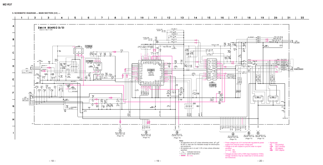
Schematic Diagram Main /3
MZ-R37
Electrical Parts List
CAP-CHIP
JFJ7001 Line in Optical
Diode MA8140-M-TX
Jack PHONES/REMOTE
Transistor XP4313-TX.SO
RES-CHIP
Network Resistor
FILTER, Chip EMI Common Mode
Filter
OP Service Assy
Electrical Parts LIST/MISCELLANEOUS Incorrect Correct
Incorrect Correct
Head ASSY, OP