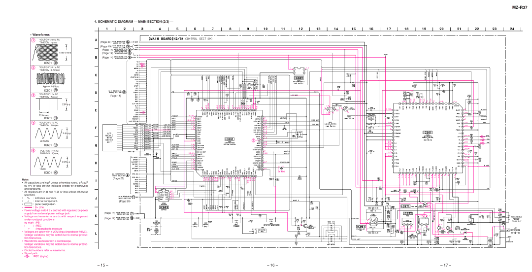
• Waveforms
1 | VOLT/DIV : 0.5V AC |
| TIME/DIV : 1μsec |
| |
| IC501 ek |
2 | VOLT/DIV : 0.1V AC |
| TIME/DIV : 0.1msec |
| Approx. |
| IC501 wl |
3 | VOLT/DIV : 1V AC |
| TIME/DIV : 5msec |
| |
| 13.4msec |
| IC601 qa |
4 | VOLT/DIV : 1V AC |
| TIME/DIV : 20nsec |
| |
| 22.5MHz |
| IC601 qj |
5 | VOLT/DIV : 1V AC |
| TIME/DIV : 20nsec |
| |
| 12kHz |
| IC801 r; |
Note:
•All capacitors are in µF unless otherwise noted. pF: µµF 50 WV or less are not indicated except for electrolytics and tantalums.
•All resistors are in Ω and 1/4 W or less unless otherwise specified.
•% : indicates tolerance.
•f : internal component.
•C : panel designation.
•A : B+ Line.
•Power voltage is dc 4.5 V and fed with regulated dc power supply from external power voltage jack.
•Voltage and waveforms are dc with respect to ground under
no mark : PB
( ) : REC
∗: Impossible to measure
•Voltages are taken with a VOM (Input impedance 10 MΩ). Voltage variations may be noted due to normal produc- tion tolerances.
•Waveforms are taken with a oscilloscope.
Voltage variations may be noted due to normal produc- tion tolerances.
•Circled numbers refer to waveforms.
•Signal path.
c : REC (digital)
MZ-R37
4. SCHEMATIC DIAGRAM — MAIN SECTION (2/3) —
(Page 20)
(Page 19) (Page 14) (Page 14)
(Page 14)
(Page 14)
(Page 20)
(Page 20)
(Page 14)
(Page 14)
– 15 – | – 16 – | – 17 – |