BIOS Setup Utility |
|
After you have completed the changes, press [Esc] and follow the
instructions on your screen to save your settings or exit without saving.
The following table describes each field in the Advanced Chipset Features
Menu and how to configure each parameter.
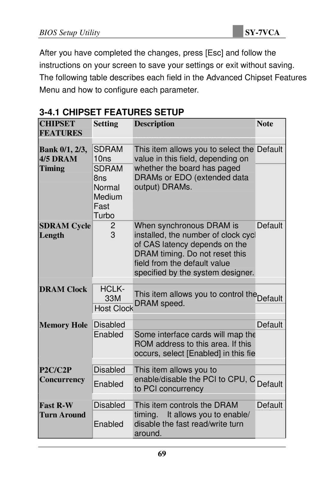
3-4.1 CHIPSET FEATURES SETUP
CHIPSET FEATURES
Bank 0/1, 2/3,
4/5 DRAM
Timing
SDRAM Cycle Length
Setting | Description | Note |
|
|
|
|
|
|
SDRAM | This item allows you to select the | Default |
10ns | value in this field, depending on |
|
SDRAM | whether the board has paged |
|
8ns | DRAMs or EDO (extended data |
|
Normal | output) DRAMs. |
|
Medium |
|
|
Fast |
|
|
Turbo |
|
|
2 | When synchronous DRAM is | Default |
3installed, the number of clock cycles of CAS latency depends on the DRAM timing. Do not reset this field from the default value specified by the system designer.
DRAM Clock
HCLK-
This item allows you to control the
33MDefault Host Clock DRAM speed.
Memory Hole
|
|
|
Disabled |
| Default |
Enabled | Some interface cards will map their |
|
| ROM address to this area. If this |
|
| occurs, select [Enabled] in this field. |
|
|
|
|
P2C/C2P Concurrency
Fast R-W Turn Around
|
|
|
Disabled | This item allows you to |
|
Enabled | enable/disable the PCI to CPU, CPU | Default |
| to PCI concurrency |
|
|
|
|
Disabled | This item controls the DRAM | Default |
| timing. It allows you to enable/ |
|
Enabled | disable the fast read/write turn |
|
| around. |
|
69