Interconnection of MSP-PRGS430 to OTP/EPROM-Based
3.6Interconnection of
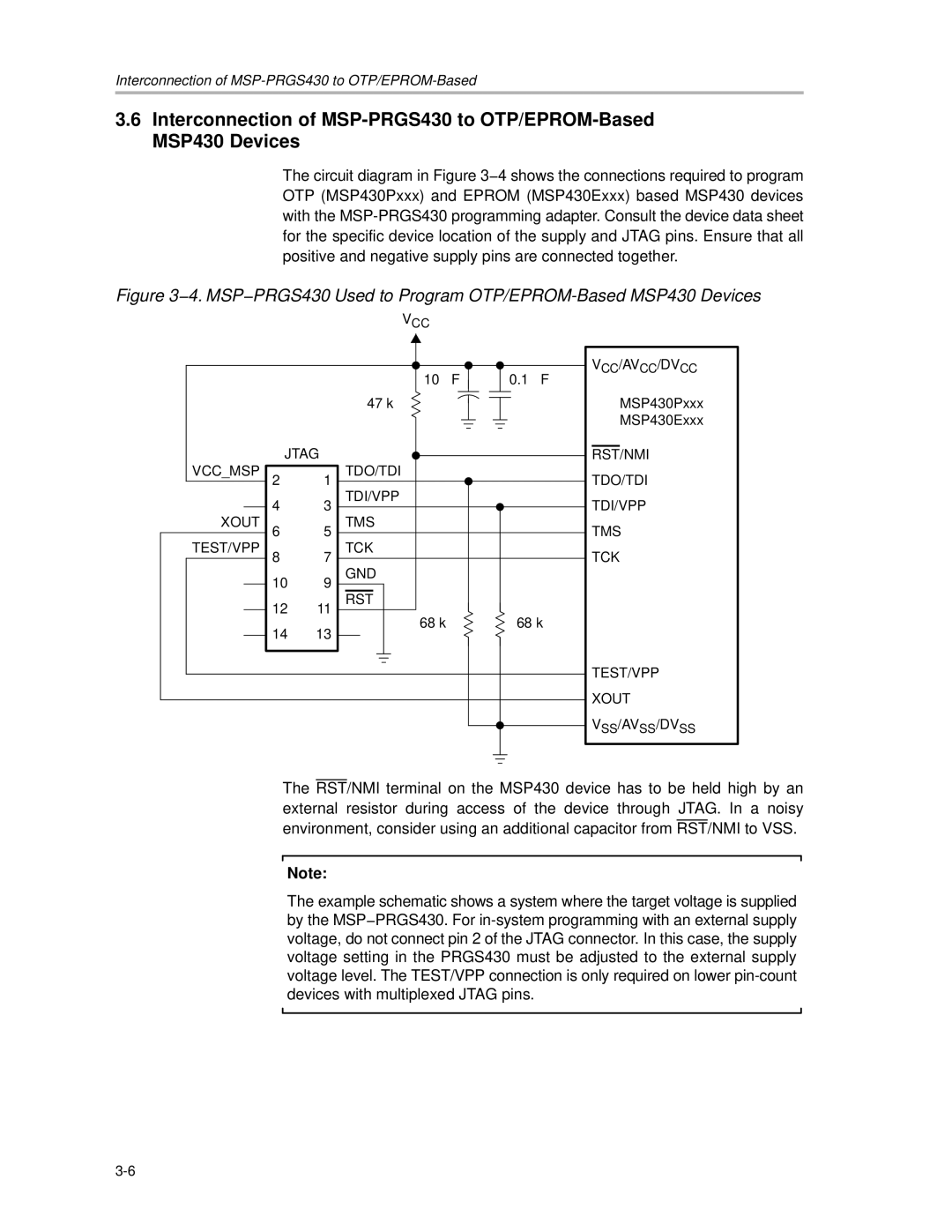
The circuit diagram in Figure 3−4 shows the connections required to program OTP (MSP430Pxxx) and EPROM (MSP430Exxx) based MSP430 devices with the
Figure 3−4. MSP−PRGS430 Used to Program OTP/EPROM-Based MSP430 Devices
VCC
|
|
|
|
|
|
|
|
|
|
|
|
|
|
|
|
|
| 10 ∝F |
|
|
|
|
|
|
|
|
| 0.1 ∝F |
| ||
|
|
|
|
|
|
|
|
|
|
|
|
|
|
|
|
|
|
|
|
|
|
|
|
|
|
|
| ||||
|
|
|
|
|
|
|
|
|
|
|
|
|
|
|
|
|
|
|
|
|
|
|
|
|
|
|
| ||||
|
|
| JTAG |
|
|
| 47 kΩ |
|
|
|
|
|
|
|
|
|
|
|
|
|
|
|
| ||||||||
|
|
|
|
|
|
|
|
|
|
|
|
|
|
|
|
|
|
|
|
|
| ||||||||||
|
|
|
|
|
|
|
|
|
|
|
|
|
|
|
|
|
|
|
|
|
|
|
|
|
|
|
|
| |||
| VCC_MSP |
| TDO/TDI |
|
|
|
|
|
|
|
|
|
|
|
|
|
|
| |||||||||||||
|
|
|
|
|
|
|
|
|
|
|
|
|
|
|
|
| |||||||||||||||
|
|
|
|
|
|
|
|
|
|
|
|
|
|
|
|
|
|
|
| ||||||||||||
| 2 | 1 |
|
|
|
|
|
|
|
|
|
|
|
| |||||||||||||||||
|
|
|
| TDI/VPP |
|
|
|
|
|
|
|
|
|
|
|
|
|
|
| ||||||||||||
|
|
| 4 | 3 |
|
|
|
|
|
|
|
|
|
|
|
|
|
|
|
| |||||||||||
|
|
|
|
|
|
|
|
|
|
|
|
|
|
|
|
|
|
|
|
|
|
|
|
|
|
|
|
| |||
| XOUT |
| TMS |
|
|
|
|
|
|
|
|
|
|
|
|
|
|
| |||||||||||||
| 6 | 5 |
|
|
|
|
|
|
|
|
|
|
|
|
|
|
|
| |||||||||||||
| TEST/VPP |
| TCK |
|
|
|
|
|
|
|
|
|
|
|
|
|
|
| |||||||||||||
| 8 | 7 |
|
|
|
|
|
|
|
|
|
|
|
|
|
|
|
| |||||||||||||
|
|
|
| GND |
|
|
|
|
|
|
|
|
|
|
|
|
|
|
| ||||||||||||
|
|
| 10 | 9 |
|
|
|
|
|
|
|
|
|
|
|
|
|
|
|
| |||||||||||
|
|
|
|
|
|
|
|
|
|
|
|
|
|
|
|
|
|
|
|
|
|
|
|
|
|
|
|
| |||
|
|
| 12 | 11 |
| RST |
|
|
|
|
|
|
|
|
|
|
|
|
|
|
|
|
|
| |||||||
|
|
|
|
|
|
|
|
|
|
|
|
|
| 68 kΩ |
|
|
|
|
|
|
|
|
|
| 68 kΩ |
| |||||
|
|
| 14 | 13 |
|
|
|
|
|
|
|
|
|
|
|
|
|
|
|
|
|
|
|
|
|
| |||||
|
|
|
|
|
|
|
|
|
|
|
|
|
|
|
|
|
|
|
|
|
|
|
|
|
|
|
|
| |||
|
|
|
|
|
|
|
|
|
|
|
|
|
|
|
|
|
|
|
|
|
|
|
|
|
|
|
|
| |||
|
|
|
|
|
|
|
|
|
|
|
|
|
|
|
|
|
|
|
|
|
|
|
|
|
|
|
|
|
|
|
|
|
|
|
|
|
|
|
|
|
|
|
|
|
|
|
|
|
|
|
|
|
|
|
|
|
|
|
|
|
|
|
|
|
|
|
|
|
|
|
|
|
|
|
|
|
|
|
|
|
|
|
|
|
|
|
|
|
|
|
|
|
|
|
|
|
|
|
|
|
|
|
|
|
|
|
|
|
|
|
|
|
|
|
|
|
|
|
|
|
|
|
|
|
|
|
|
|
|
|
|
|
|
|
|
|
|
|
|
|
|
|
|
|
|
|
|
|
|
|
|
|
|
|
|
|
|
|
|
|
|
|
|
|
|
|
|
|
|
|
|
|
|
|
|
|
|
|
|
|
|
|
|
|
|
|
|
|
|
|
|
|
|
|
|
|
|
|
|
|
|
|
|
|
|
|
|
|
|
|
|
|
|
|
|
|
|
|
|
|
|
|
|
|
|
|
|
|
|
|
|
|
|
|
|
|
|
|
|
|
|
|
|
|
|
|
|
|
|
|
|
|
|
|
|
|
|
|
|
|
|
|
|
|
|
|
|
|
|
|
|
|
|
|
|
|
|
|
|
|
|
|
|
|
|
|
|
|
|
|
|
|
|
|
|
|
|
|
|
|
|
|
|
|
|
|
|
|
|
|
|
|
|
|
|
|
|
|
|
VCC/AVCC/DVCC
MSP430Pxxx
MSP430Exxx
RST/NMI
TDO/TDI
TDI/VPP
TMS
TCK
TEST/VPP
XOUT
VSS/AVSS/DVSS
The RST/NMI terminal on the MSP430 device has to be held high by an external resistor during access of the device through JTAG. In a noisy environment, consider using an additional capacitor from RST/NMI to VSS.
Note:
The example schematic shows a system where the target voltage is supplied by the MSP−PRGS430. For